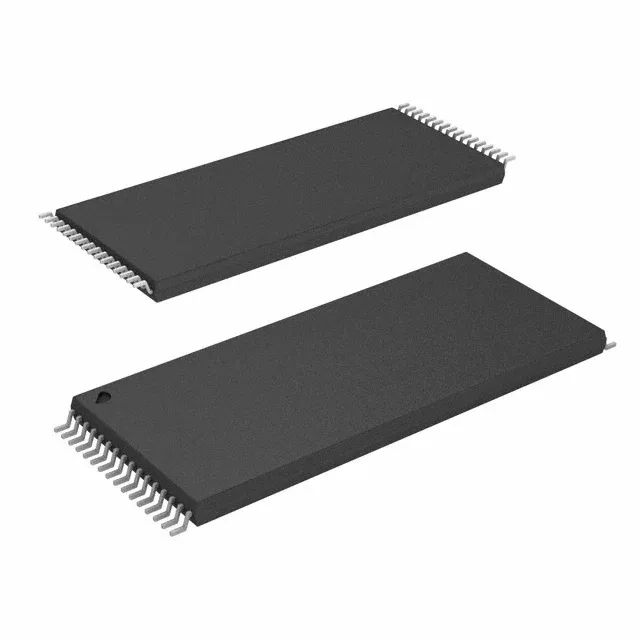
The AT28C010-15TU-T: That means it remains a valid line-item for current production BOMs and new designs, with no forced migration timeline. No stock-holding claim is made here.
What 150 ns access time means for bus timing
The 150 ns access time is the maximum delay from address valid to data valid on the parallel bus. For a microcontroller running at 8 MHz with a 125 ns bus cycle, this part meets the setup timing with margin — the CPU inserts one wait state per read cycle. At 10 MHz (100 ns cycle), two wait states are needed, which halves the effective read throughput to ~5 MB/s. The parallel interface means all 8 data lines and the address bus are driven directly — no serial protocol overhead. This suits systems where the memory bus is already routed for SRAM or NOR flash and the designer needs non-volatile storage without a SPI/I²C translation layer.
Memory organization and write cycle timing
Organized as 128K x 8 bits, the full 1 Mbit array is byte-addressable. The 10 ms write cycle time per word or page means a full-chip rewrite of 128 KB takes roughly 21 minutes if written byte-by-byte — page-mode writes reduce this significantly. The part does not operate at 3.3 V; a level translator or separate 5 V regulator is required if the rest of the board runs on a lower core voltage. This covers most factory-floor, outdoor telecom, and automotive cabin applications.
Compliance and documentation
RoHS3 compliant — no restricted substances above the threshold limits. The manufacturer provides a full material declaration and REACH compliance data upon request through the standard documentation portal.