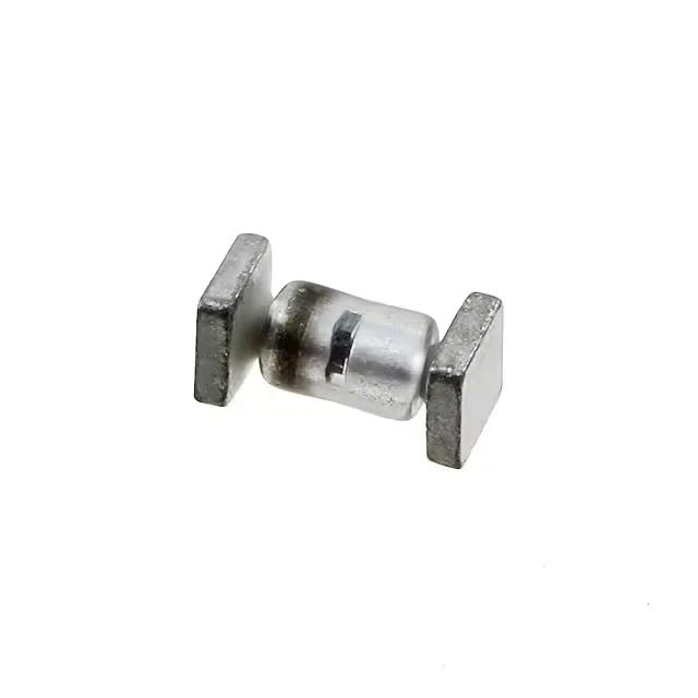
The 1N6311US is a 3 V nominal Zener diode from Microchip Technology, rated at 500 mW maximum power dissipation. The ±5% tolerance on the Zener voltage means the regulation point sits between 2.85 V and 3.15 V at the specified test current — tight enough for most reference and clamping duties in low-voltage rail protection or bias generation. Maximum Zener impedance (Zzt) is 29 Ohms. A lower impedance means tighter regulation as the current changes; at 29 Ohms the 1N6311US holds the output within roughly 29 mV per mA of load variation, which is adequate for general-purpose clamping and simple shunt regulators where the load current is stable. Reverse leakage is specified at 30 µA maximum when 1 V is applied across the device. For a 3 V Zener this is a low leakage figure — the junction starts conducting well below the breakdown knee, so the part draws negligible current in circuits where the rail stays under 2 V.
Package, temperature range, and deployment context
Housed in the SQ-MELF B package (surface-mount MELF, B-size), the 1N6311US is a hermetic ceramic package with metalized end caps. The MELF form factor is common in high-reliability and military/aerospace designs where the hermetic seal prevents moisture ingress and the cylindrical body handles thermal cycling better than molded plastic SOD-123 or SOT-23 packages. At 175°C junction temperature the 500 mW power rating must be derated per the device's thermal resistance; in practice this part is suited for avionics, downhole instrumentation, and engine-bay electronics where ambient temperatures exceed 125°C. The forward voltage spec — 1.4 V maximum at 1 A forward current — confirms the die can handle short forward-current surges during reverse-polarity events or inductive kickback. The 1 A peak forward current is higher than the continuous Zener current at 500 mW (roughly 167 mA at 3 V), so the part survives brief forward overstress without failing short.