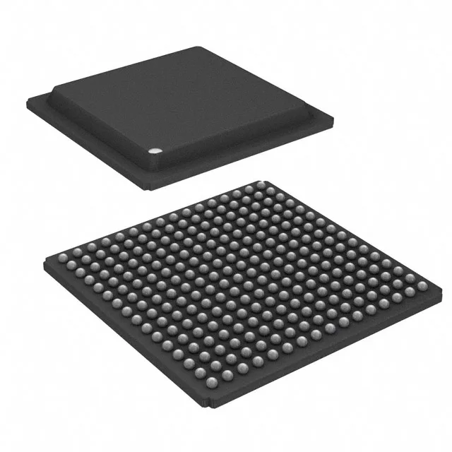
Lattice Semiconductor Corporation LCMXO2280C-4FTN256C — FPGA / CPLD & Programmable Logic

LCMXO2280C-4FTN256C Lattice MachXO FPGA, 2280 LEs, 211 I/O

MPNLCMXO2280C-4FTN256C
Active

Lattice Semiconductor MachXO FPGA, LCMXO2280C-4FTN256C, 2280 logic elements, 211 I/O, 28262 bits SRAM, 1.71V–3.465V supply, 256-FTBGA, 0°C to 85°C, Tray.

$41.9000Ref. price · indicative, final on quote
Packaging256-LBGA
RoHSROHS3 Compliant
SeriesMachXO
Independent supplier — new & surplus stockAuthenticity-screened · ESD-safe packingListing updated Aug 2026

Specifications

LCMXO2280C-4FTN256C specifications
ParameterValue
SeriesMachXO
MountingSurface Mount
Supply voltage1.71V ~ 3.465V
Operating temperature0°C ~ 85°C (TJ)
PackageTray
Number of i (O)211
Case256-LBGA
Total RAM bits28262
Number of LABs (CLBs)285
Number of logic elements (Cells)2280

Product details

2280 logic elements, 211 I/O in a 256-ball BGA

The LCMXO2280C-4FTN256C is a Lattice MachXO FPGA packing 2280 logic elements (285 LABs/CLBs) and 28262 bits of distributed SRAM, enough for moderate glue-logic, bus bridging, or control-state machines that need on-chip register storage without an external SRAM. Its 211 user I/O in a 256-ball FTBGA (17x17 mm) gives a high pin-to-package ratio — useful for designs that need many parallel signals in a compact footprint, though the 0.8 mm ball pitch demands careful fan-out on a 4-layer board.

ROHS3 compliant. The part ships in a Tray, surface-mount to the 256-FTBGA footprint.

Frequently asked questions

When sourcing LCMXO2280C-4FTN256C, what is the closest functional alternative — LCMXO2280C-3FTN256C?

The LCMXO2280C-3FTN256C shares the same die, package (256-FTBGA), I/O count (211), and memory (28262 bits SRAM) — the only difference is the speed grade: -4 is faster than -3. The -3 variant is a drop-in replacement for the same PCB footprint and BOM position if the timing closure allows the slower grade.