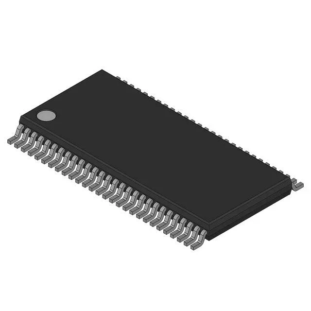
Intel DE28F800F3T115 — Analog & Data Acquisition

DE28F800F3T115 Flash Memory, 8Mbit 115ns Boot Block 56-SSOP

MPNDE28F800F3T115
End of Life

Intel DE28F800F3T115, 8Mbit Non-Volatile FLASH - Boot Block, 512K x 16 organization, 115 ns access time, CUI interface, 3V ~ 3.6V supply, -40°C ~ 125°C TA, 56-SOP/56-SSOP surface mount package.

$4.0Ref. price · indicative, final on quote
Packaging56-SOP
StockContact for availability
MOQ1 pcs
  • 100% new & originalTraceable channels only — no refurbs, no pulls, no remarked parts.
  • Date & lot codes on quoteStated per line before you commit; label photos on request.
  • MSL-compliant ESD packingMoisture-sealed bags with indicator cards; reels photo-verified.
  • PayPal buyer protectionPay by T/T, PayPal or Payoneer — card payments covered end to end.

Specifications

DE28F800F3T115 Technical Specifications
ParameterValue
Memory typeNon-Volatile
Mounting typeSurface Mount
Voltage3V ~ 3.6V
Memory interfaceCUI
Operating temperature-40°C ~ 125°C (TA)
PackageBulk
TechnologyFLASH - Boot Block
Access time115 ns
Memory size8Mbit
Memory formatFLASH
Case56-SOP
Memory organization512K x 16
Write cycle time - word, page200µs

Product details

8Mbit boot-block Flash for harsh-environment firmware storage

The Intel DE28F800F3T115 is an 8Mbit boot-block Flash memory organized as 512K x 16, with a 115 ns access time and a Common User Interface (CUI) for command-driven read/write operations. The boot-block architecture provides hardware-protected sectors for critical boot code, preventing accidental corruption during power-loss or incomplete writes — a feature that matters for embedded systems where the CPU must come up cleanly after a brownout. Rated for -40°C to 125°C operation, this part is suited for industrial motor drives, automotive under-hood controllers, and avionics data-logging modules where the ambient temperature exceeds standard commercial limits.

115 ns access time — what it means for bus timing

The 115 ns access time is the window from address assertion to valid data on the bus. Write cycle time is 200 µs per word or page.

Boot Block architecture and field-reprogramming

Boot-block Flash partitions the memory array into independently lockable sectors, with the boot block (typically the lowest address range) protected by a hardware write-lock mechanism. This prevents a runaway firmware update from bricking the system — the bootloader stays intact even if the application sector is corrupted mid-write. The CUI command set follows the industry-standard 12V-block erase/program algorithm, so existing firmware drivers for Intel 28F-series Flash should port with minimal changes. No field-reprogramming via UART or JTAG is built in; the host CPU manages all erase and program sequences through the parallel interface.

Package and temperature grade — where it fits physically

Housed in a 56-SSOP surface-mount package, this part operates from -40°C to 125°C and from 3V to 3.6V.

Frequently asked questions

What is the DE28F800F3T115 memory access time?

The DE28F800F3T115 has a 115 ns access time, which is the time from address assertion to valid data on the bus.

What is the operating temperature range for DE28F800F3T115?

The DE28F800F3T115 is rated for -40°C to 125°C ambient temperature operation, covering industrial and automotive extended-temperature environments.