25,000 logic elements — sizing the gate budget
The 25,000 LE count (1563 LABs/CLBs) defines the upper bound for combinatorial and sequential logic you can fit without external CPLD or glue logic. For a typical motor-control encoder interface or a multi-axis position-latch block, this density leaves headroom for a small state machine and a UART bridge alongside the primary datapath.
178 I/O in a 256-FBGA — routing and footprint
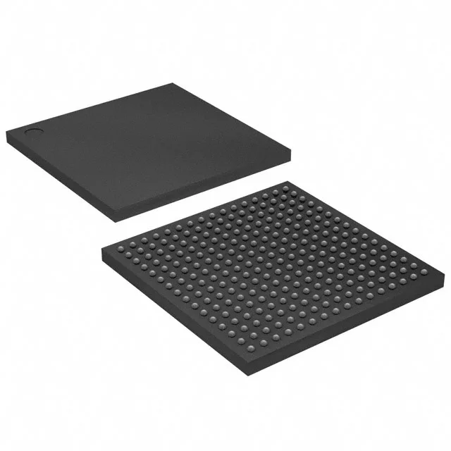
The 256-FBGA (17x17 mm) body routes 178 user I/O. That is a dense pinout for the package size — expect four to six signal layers on the PCB to escape the BGA balls cleanly. The remaining balls are core supplies, configuration pins, and dedicated clock inputs. If your design needs more than 178 I/O, the 484-ball sibling (10M25DAF484I6G) offers 360 I/O in the same logic-density tier.
Industrial temperature range — no derating surprise
The 100°C TJ limit means the case temperature must stay lower — factor in the FPGA's dynamic power dissipation and enclosure airflow when calculating the thermal budget.
No last-time-buy or end-of-life notice applies. For dual-sourcing or a higher-I/O variant, the 10M25DAF484I6G (360 I/O, same 25K LE and RAM) is a functional peer in the same MAX 10 family, though the package differs.