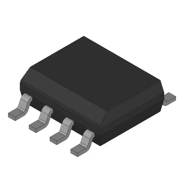
The W194-70G is a frequency multiplier and zero delay buffer. Maximum output frequency is 133 MHz with a 2:2 input-to-output ratio, operating from 0°C to 70°C.
Dual supply range: 3.3V or 5V
The supply voltage range covers both 3.3V nominal (3.135V–3.465V) and 5V nominal (4.5V–5.5V), so the same part can be used in a 3.3V core logic board or a legacy 5V peripheral bus. No external level translation needed on the supply.
RoHS non-compliant — legacy finish
The W194-70G is RoHS non-compliant with a lead-bearing finish.
Housed in an 8-pin SOIC (0.154" body width, 3.90 mm pitch), surface-mount. The 8-SOIC footprint is a standard, hand-solderable package — easy to prototype on a breakout board or integrate into a production PCB. No exposed pad, no thermal vias needed.