Infineon Technologies W152-1G — Clock & Timing ICs

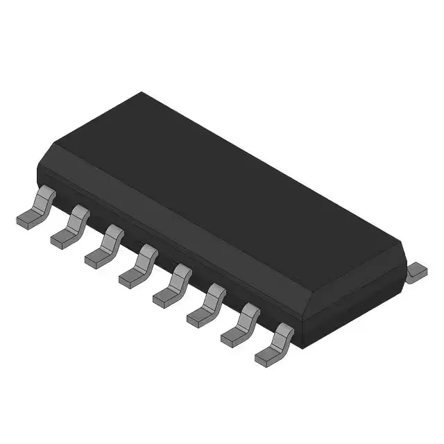
W152-1G Zero Delay Buffer, PLL, 140 MHz, 16-SOIC

MPNW152-1G
End of Life

Spread Aware™ series, Zero Delay Buffer, PLL Yes, 1:8 fanout, 140 MHz max, 2.97V–3.63V supply, 16-SOIC, 0°C to 70°C.

$3.27Ref. price · indicative, final on quote
Packaging16-SOIC (0.154", 3.90mm Width)
StockContact for availability
MOQ1 pcs
  • 100% new & originalTraceable channels only — no refurbs, no pulls, no remarked parts.
  • Date & lot codes on quoteStated per line before you commit; label photos on request.
  • MSL-compliant ESD packingMoisture-sealed bags with indicator cards; reels photo-verified.
  • PayPal buyer protectionPay by T/T, PayPal or Payoneer — card payments covered end to end.

Specifications

W152-1G Technical Specifications
ParameterValue
TypeZero Delay Buffer
SeriesSpread Aware™
Mounting typeSurface Mount
Voltage2.97V ~ 3.63V
Frequency140MHz
Operating temperature0°C ~ 70°C (TA)
PLLYes
PackageBulk
Case16-SOIC (0.154\", 3.90mm Width)
Divider (Multiplier)Yes/No
Number of circuits1
Ratio - Input:Output1:8
Differential - Input:OutputNo/No

Product details

What the W152-1G does on the clock tree

The W152-1G is a PLL-based zero delay buffer from the Spread Aware™ family, designed to regenerate and distribute a single reference clock to eight outputs with near-zero propagation delay. Its integrated PLL locks to the input and aligns the output edges, making it a fit for synchronous clock domains in networking gear, base stations, and test equipment where skew between multiple loads must be minimized. The 1:8 fanout covers most multi-load clock trees without needing external fanout buffers, and the 140 MHz ceiling handles Gigabit Ethernet, PCIe reference clocks, and mid-speed FPGA interfaces.

Supply rail and temperature — where it fits

The supply range is 2.97 V to 3.63 V, which maps to a regulated 3.3 V rail with ±10% tolerance. This is a narrow-range part — do not feed it from a 2.5 V or 5 V supply without a regulator. The operating temperature covers 0°C to 70°C, the commercial grade, limiting the W152-1G to indoor, temperature-controlled environments such as server rooms, telecom central offices, or lab instruments. For industrial enclosures or outdoor cabinets, a wider-temperature zero delay buffer would be needed.

Package and footprint

Housed in a 16-SOIC with 3.90 mm body width, the W152-1G uses a standard surface-mount footprint shared by many SOIC-16 logic and clock parts. The package is small enough for dense layouts but large enough for manual rework. No exposed pad — thermal dissipation is through the leads and board copper.

RoHS non-compliance — what it means for the BOM

The W152-1G is RoHS non-compliant, meaning it contains lead (Pb) above the 0.1% threshold. This triggers an exemption declaration under EU RoHS Directive 2011/65/EU and similar regulations in China, Korea, and California. If your design targets a lead-free assembly line or must meet full RoHS compliance, this part adds paperwork and may be rejected by your CM. For military, aerospace, or high-reliability applications where leaded solder is still preferred or exempted, this is not a blocker.

Lifecycle and sourcing posture

That means no last-time-buy scramble and no forced redesign for the foreseeable future. For dual-sourcing or a second-source evaluation, the CY2305SXI-1HT from Cypress offers a similar zero delay buffer function with 1:5 fanout and industrial temperature range, but verify pin compatibility against your layout before substituting.

Frequently asked questions

What package does the W152-1G use?

The W152-1G is supplied in a 16-SOIC package with a 3.90 mm body width, surface-mount. The supplier device package is 16-SOIC.

What is a functional second-source for the W152-1G?

The Cypress CY2305SXI-1HT is a close functional peer — also a PLL-based zero delay buffer, but with 1:5 fanout and industrial temperature range (-40°C to 85°C) versus the W152-1G's 1:8 and commercial range. Verify pin compatibility before substituting.