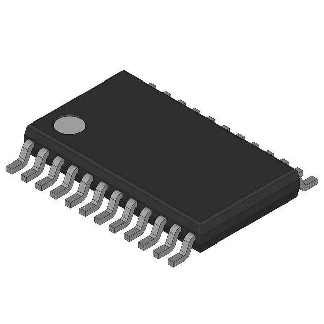
Infineon Technologies W132-10BXT — Clock & Timing ICs

W132-10BXT Zero Delay Buffer, PLL, 140 MHz, 24-TSSOP

MPNW132-10BXT
End of Life

W132-10BXT, Spread Aware™ series, Zero Delay Buffer with PLL, 140 MHz max, 2:11 input:output, LVCMOS/LVTTL outputs, 2.97V–3.63V supply, 0°C to 70°C, 24-TSSOP surface mount.

$1.0Ref. price · indicative, final on quote
Packaging24-TSSOP (0.173", 4.40mm Width)
StockContact for availability
MOQ1 pcs
  • 100% new & originalTraceable channels only — no refurbs, no pulls, no remarked parts.
  • Date & lot codes on quoteStated per line before you commit; label photos on request.
  • MSL-compliant ESD packingMoisture-sealed bags with indicator cards; reels photo-verified.
  • PayPal buyer protectionPay by T/T, PayPal or Payoneer — card payments covered end to end.

Specifications

W132-10BXT Technical Specifications
ParameterValue
TypeZero Delay Buffer
SeriesSpread Aware™
Mounting typeSurface Mount
Voltage2.97V ~ 3.63V
Frequency140MHz
Operating temperature0°C ~ 70°C (TA)
PLLYes
InputClock
OutputLVCMOS, LVTTL
PackageBulk
Case24-TSSOP (0.173\", 4.40mm Width)
Divider (Multiplier)No/No
Number of circuits1
Ratio - Input:Output2:11
Differential - Input:OutputNo/No

Product details

What this clock buffer does on the board

The W132-10BXT is a PLL-based zero delay buffer from the Spread Aware™ series, designed to regenerate a clock input with deterministic phase alignment and fan it out to multiple loads. It accepts a single-ended clock input and produces up to eleven LVCMOS or LVTTL outputs at frequencies up to 140 MHz, with a 2:11 input-to-output ratio. The zero-delay architecture means the output edges align to the input within the PLL's capture range, making it suitable for synchronising multiple ICs on a single PCB without adding skew.

140 MHz ceiling and what it means for your clock tree

The maximum frequency is 140 MHz. The PLL locks to the input frequency; divider/multiplier is No/No, so output frequency equals input.

2:11 fanout — eleven clock lines from two reference inputs

The 2:11 ratio means two clock input pins feed eleven output pins. In practice you drive one input and leave the other as a redundant or alternate reference, or use the second input for a different clock domain if the PLL can switch between them. The eleven outputs give you enough fanout for a moderate-sized board with multiple FPGAs, ASICs, or memory banks without adding a second buffer. The outputs are non-differential — single-ended LVCMOS or LVTTL only — so long PCB traces above a few inches need impedance matching and possibly series termination to maintain signal integrity at 140 MHz.

Supply rail and temperature — fit for the environment

The supply range is 2.97 V to 3.63 V. The operating temperature range is 0°C to 70°C.

Package and mounting — 24-TSSOP surface mount

The 24-TSSOP package has a 0.173-inch body width and 4.40 mm footprint. The supplier device package is 24-TSSOP.

Lifecycle and sourcing — active, no end-of-life watch

The W132-10BXT carries an Active product status. No NRND or last-time-buy flags appear on the lifecycle record. For a BOM line that needs a zero-delay clock buffer, this part does not carry the supply-chain risk of an end-of-life part.

Provenance check — what to look for on the markings

The 24-TSSOP package uses laser-etched date codes and lot numbers. Verify the top-mark font matches the manufacturer's standard for the Spread Aware series.

Frequently asked questions

What is the maximum frequency of W132-10BXT?

The maximum operating frequency is 140 MHz. Output frequency equals the input frequency because the divider/multiplier is set to No/No.

What is W132-10BXT's listed type on this component line?

The listed type is Zero Delay Buffer, and it includes a PLL. The input is a clock signal, and the outputs are LVCMOS or LVTTL.