Fixed 3.3 V rail for automotive always-on domains
The TLS203B0EJV33XUMA1 is a single-output LDO from Infineon's OPTIREG family, delivering a fixed 3.3 V at up to 300 mA. The 20 V maximum input covers a 12 V automotive battery with load-dump margin — the internal pass element survives the transient without an external clamp. Dropout is 0.4 V max at full load, so a 3.6 V pre-regulator rail keeps the output in regulation across the temperature range. The 60 µA quiescent current keeps the always-on domain draw low enough for battery-backed modules that must wake on a CAN or LIN message.
PSRR and noise rejection for sensitive loads
Power-supply rejection ratio is 65 dB at 120 Hz — this is the ripple frequency from a full-wave rectified 60 Hz mains, but it also tells you the regulator's ability to reject alternator whine and DC-DC switching ripple in the audio band. At 65 dB, a 100 mVpp ripple on the input is attenuated to roughly 56 µVpp at the output. The Enable pin lets the system microcontroller gate the output during sleep modes, dropping the total supply current to the 60 µA quiescent level plus the load on the VIN pin. Protection includes over-current, over-temperature, and reverse polarity — the reverse-polarity block prevents damage if the battery leads are swapped during service, a common field failure in automotive modules.
PG-DSO-8-27 package and thermal management
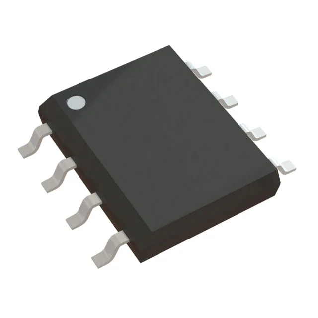
The 8-pin SOIC package with exposed pad (PG-DSO-8-27) routes the die's heat through the paddle to the PCB copper plane. For 300 mA output at 3.3 V from a 5 V input, the power dissipation is roughly 0.51 W — the exposed pad soldered to a 1 in² copper area on a 2-layer board keeps the junction temperature below 125 °C in a 85 °C ambient. The datasheet's thermal resistance figure (junction-to-ambient) assumes the recommended PCB footprint; the actual RthJA depends on the copper area and the number of thermal vias under the pad.