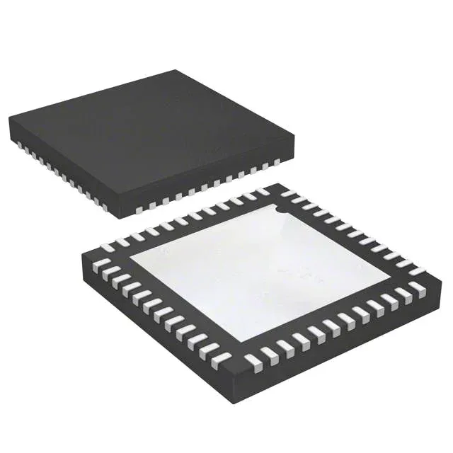
Motor-drive SoC with Cortex-M3 and LIN
The TLE9867QXA40XUMA2 is an automotive-grade motor driver system-on-chip from Infineon, integrating an ARM Cortex-M3 core, 64 kB flash, 6 kB RAM, and a LIN transceiver in a single VQFN-48 package. The part is classified under Interface & Transceivers but functions as a complete embedded motor-control node — the Cortex-M3 runs the control algorithm, the on-chip flash holds the firmware, and the LIN interface handles the vehicle bus communication. The AEC-Q100 qualification (Grade 0 implied by the 150 °C rating) means the part has passed the full automotive reliability stress suite — extended temperature cycling, high-temperature operating life, and ESD robustness per the AEC specification.
Memory and I/O budget for the control loop
64 kB of on-chip flash is sufficient for a sensorless field-oriented control (FOC) library plus the LIN stack and diagnostic routines. The 6 kB RAM (organized as 6K x 8) holds the rotor-flux observer state variables, current-regulation PI terms, and a small data buffer for the UART debug interface — budget the RAM allocation before committing to the firmware architecture. Ten general-purpose I/O lines are available for hall-effect sensor inputs, brake-pWM outputs, fault indicators, or a secondary SPI slave. With the LIN, SSI, and UART interfaces consuming at least three pins for the serial buses, the remaining I/O count is tight — a design using four hall inputs and two fault outputs leaves only one spare pin.
Package thermal management at 150 °C junction
The 48-VFQFN exposed-pad package (supplier device package VQFN-48-31) requires a thermal-via array under the center pad to conduct heat into the PCB ground plane. With a 150 °C maximum junction temperature and the motor-driver output stage dissipating several watts during stall conditions, the board layout must provide a low-thermal-resistance path — a 2x2 array of 0.3 mm vias under the pad is the minimum for survival at the temperature extreme. The surface-mount package is supplied in Tape & Reel (TR) or Cut Tape (CT) options, suitable for high-volume reflow assembly.