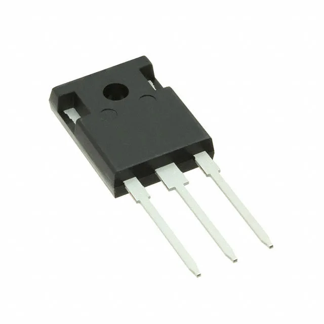
650 V CoolMOS for hard-switching PFC and inverter stages
The SPW35N60C3FKSA1: This is a first-generation CoolMOS device from the C3 series, designed for hard-switching topologies where low conduction loss and fast switching are both required.
Total gate charge is 200 nC at a 10 V gate drive. Input capacitance is 4500 pF at 25 V drain-source — this dominates the Coss energy stored per cycle and contributes to the turn-off loss in hard-switched bridges.
Thermal and package reality for the BOM
Maximum power dissipation is 313 W at the case — this is the theoretical limit with an ideal heatsink; the real-world dissipation is set by the junction-to-case thermal resistance and the heatsink's ability to hold the case temperature below 150 °C at the target load current. The TO-247-3 package (PG-TO247-3-1) provides a large copper tab for heat extraction and is suited for bolted mounting to a heatsink with thermal interface material — the through-hole leads handle the high current without PCB trace bottlenecks. The 3.9 V maximum gate threshold at 1.9 mA drain current means a standard 10 V gate drive fully enhances the channel.
Lifecycle and compliance posture
ROHS3 compliant per the manufacturer's declaration — no exemption expiry concerns for current designs.