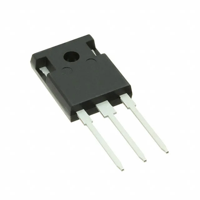
Infineon Technologies SPW17N80C3FKSA1

Infineon SPW17N80C3FKSA1 CoolMOS N-Ch MOSFET, 800V 17A

MPNSPW17N80C3FKSA1
End of Life

Infineon CoolMOS™ SPW17N80C3FKSA1 N-channel MOSFET, 800 V drain-source, 17 A continuous drain, 290 mOhm Rds(on) at 10 V gate drive, TO-247-3 through-hole package, -55°C to 150°C junction temperature.

$5.24Ref. price · indicative, final on quote
PackagingTO-247-3
StockContact for availability
MOQ1 pcs
  • 100% new & originalTraceable channels only — no refurbs, no pulls, no remarked parts.
  • Date & lot codes on quoteStated per line before you commit; label photos on request.
  • MSL-compliant ESD packingMoisture-sealed bags with indicator cards; reels photo-verified.
  • PayPal buyer protectionPay by T/T, PayPal or Payoneer — card payments covered end to end.

Specifications

SPW17N80C3FKSA1 Technical Specifications
ParameterValue
SeriesCoolMOS™
FET typeN-Channel
Mounting typeThrough Hole
Drain to source voltage800 V
Drive voltage (Max rds on, min rds on)10V
Current - continuous drain (Id) @ 25°C17A (Tc)
Power dissipation227W (Tc)
Operating temperature-55°C ~ 150°C (TJ)
PackageTube
Vgs±20V
TechnologyMOSFET (Metal Oxide)
CaseTO-247-3
Vgs(th) (Max) @ id3.9V @ 1mA
Rds on (Max) @ id, vgs290mOhm @ 11A, 10V
Gate charge (Qg) (Max) @ vgs177 nC @ 10 V
Input capacitance (Ciss) (Max) @ vds2320 pF @ 25 V

Product details

290 mOhm on-resistance — the conduction loss number

That 290 mOhm at 11 A is the number to use for worst-case conduction loss in the thermal loop — at 17 A the I²R loss hits about 84 W, which is within the 227 W dissipation limit but leaves little margin for switching losses in a hard-switched topology. The 10 V drive voltage is typical for standard gate-driver ICs; the part also accepts up to ±20 V on the gate for noise margin in noisy environments.

177 nC gate charge — switching-speed budget

Total gate charge is 177 nC at 10 V. That's a moderate Qg for an 800 V, 17 A device — expect a gate-driver capable of sourcing at least 1 A peak to keep switching transitions under 200 ns. The 2320 pF input capacitance at 25 V drain-source confirms the gate-driver output impedance matters; a 10 Ω gate resistor is a typical starting point for ringing control without excessive turn-on delay.

Frequently asked questions

What is the SPW17N80C3FKSA1 datasheet and its key specifications?

Design engineers need to validate fit and compare electrical parameters before adoption.

Where can I buy SPW17N80C3FKSA1 and what is the price?

Sourcing buyers need to know availability and cost for procurement decisions.

Is SPW17N80C3FKSA1 still in production or obsolete?

Maintenance techs and brokers need lifecycle status for replacement planning.

What are the direct equivalents or substitutes for SPW17N80C3FKSA1?

Designers and buyers seek alternative parts for second sourcing or price optimization.

What is the SPW17N80C3FKSA1 pinout and package outline?

Techs replacing a failed unit need to confirm physical fit and pin compatibility.

What is the typical lead time for SPW17N80C3FKSA1 from major distributors?

Procurement planners need to schedule production and avoid delays.