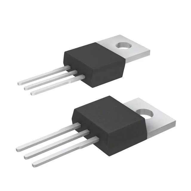
600 V CoolMOS in a TO-220 — primary-side switching workhorse
This is the conduction-loss floor at the rated current — actual Rds(on) rises with junction temperature, so the thermal budget needs headroom above the 25°C datasheet value. Total gate charge is 114 nC at 10 V. Input capacitance (Ciss) is 2400 pF at 25 V drain-source. This value, combined with the gate charge, sets the switching energy per cycle and influences the driver's turn-on and turn-off times.
Thermal and temperature envelope
The 150°C max junction is typical for CoolMOS and allows high-density power conversion, but the thermal resistance from junction to case must be managed with a proper heatsink and thermal interface material.
It is a current-production Infineon CoolMOS part, ROHS3 compliant.