Conduction and switching parametrics
Input capacitance is 1660 pF at 25 V drain-source, which together with the gate charge defines the drive current needed from the gate driver IC. The gate threshold voltage is specified at 3.9 V maximum at 675 µA, so a 10 V drive rail provides healthy overdrive for minimum Rds(on). This wide Tj window suits applications with high ambient temperatures or significant self-heating, such as enclosed power supplies or motor drives.
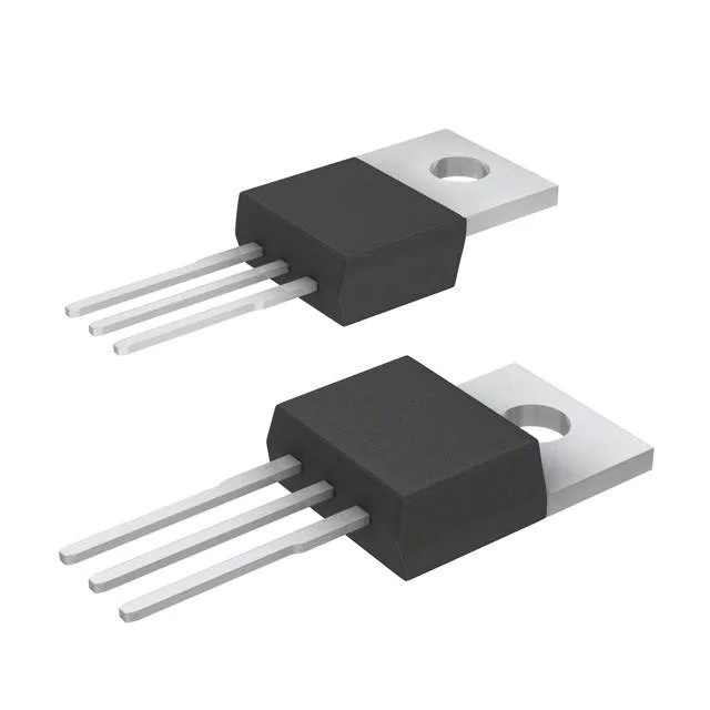
The through-hole leads require a 0.8 mm to 1.0 mm PCB hole diameter and benefit from a heatsink attached to the tab with a thermal interface material. For vibration-prone environments, mechanical support via a screw or clip is recommended.