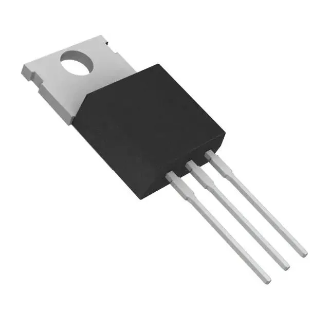
Infineon Technologies SPP08N50C3XKSA1 — Logic ICs

Infineon SPP08N50C3XKSA1 CoolMOS N-Ch MOSFET, 560 V, 7.6 A

MPNSPP08N50C3XKSA1
End of Life

Infineon CoolMOS™ SPP08N50C3XKSA1, N-Channel MOSFET, 560 V Vds, 7.6 A Id, 600 mOhm Rds(on) @ 10 V, 32 nC Qg, TO-220-3, -55 to 150 °C.

$0.85Ref. price · indicative, final on quote
PackagingTO-220-3
StockContact for availability
MOQ1 pcs
  • 100% new & originalTraceable channels only — no refurbs, no pulls, no remarked parts.
  • Date & lot codes on quoteStated per line before you commit; label photos on request.
  • MSL-compliant ESD packingMoisture-sealed bags with indicator cards; reels photo-verified.
  • PayPal buyer protectionPay by T/T, PayPal or Payoneer — card payments covered end to end.

Specifications

SPP08N50C3XKSA1 Technical Specifications
ParameterValue
SeriesCoolMOS™
FET typeN-Channel
Mounting typeThrough Hole
Drain to source voltage560 V
Drive voltage (Max rds on, min rds on)10V
Current - continuous drain (Id) @ 25°C7.6A (Tc)
Power dissipation83W (Tc)
Operating temperature-55°C ~ 150°C (TJ)
PackageBulk
Vgs±20V
TechnologyMOSFET (Metal Oxide)
CaseTO-220-3
Vgs(th) (Max) @ id3.9V @ 350µA
Rds on (Max) @ id, vgs600mOhm @ 4.6A, 10V
Gate charge (Qg) (Max) @ vgs32 nC @ 10 V
Input capacitance (Ciss) (Max) @ vds750 pF @ 25 V

Product details

560 V CoolMOS for offline power stages

The Infineon SPP08N50C3XKSA1 is an N-channel CoolMOS power MOSFET in a through-hole TO-220-3 package (PG-TO220-3-1). The 32 nC typical gate charge at 10 V keeps switching losses manageable in hard-switched topologies like flyback converters, PFC boost stages, and auxiliary power supplies where the 560 V breakdown provides margin for universal AC input designs.

The 600 mOhm max on-resistance at 10 V drive and 4.6 A sets the conduction loss baseline. At 7.6 A full load, expect roughly 600 mOhm × (7.6 A)² ≈ 35 W conduction loss — which consumes nearly half the 83 W dissipation limit at Tc=25°C. For hard-switching above 100 kHz, the 750 pF input capacitance at 25 V drain-source means the driver must supply about 75 nC per cycle at 10 V; budget gate drive losses accordingly.

Active lifecycle — no near-term LTB concern

There is no announced last-time-buy or end-of-life notice for this CoolMOS C3 series variant. For production BOMs that require a second-source hedge, the TO-220-3 footprint is common across the 500–600 V CoolMOS family, though no official cross-reference is listed in this record.

Frequently asked questions

What is the exact Vds for SPP08N50C3XKSA1?

The drain-to-source voltage rating (Vdss) is 560 V. This is the maximum voltage the MOSFET can block between drain and source with the gate shorted to source.