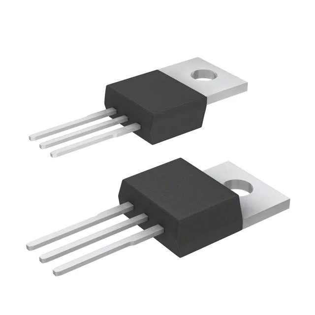
800 V CoolMOS in a TO-220 — the off-line SMOS workhorse
It is built for hard-switching topologies in power supplies, PFC stages, and flyback converters where the primary-side voltage rail exceeds 400 V. The through-hole TO-220-3 package (PG-TO220-3) keeps the thermal path to the heatsink short — the exposed metal tab is the drain, and the package handles 63 W dissipation at the case. For a bench rework standpoint, the three-lead TO-220 is about as rework-friendly as it gets: the leads are thick enough to survive a couple of desolder cycles, and the tab is easy to clamp for thermal management.
Maximum on-resistance is 1.3 Ohm at 2.5 A drain current with 10 V gate drive. At 25 °C junction, that is the conduction-loss floor; expect the resistance to roughly double at 125 °C junction, so the steady-state thermal design should budget for a hot Rds(on) around 2.6 Ohm. The 31 nC figure means a standard gate driver with 1 A peak output can switch this FET in under 50 ns, keeping crossover losses manageable at 100 kHz switching frequencies.
Temperature range and junction limits
The 150 °C absolute maximum junction sets the derating curve — continuous operation above 125 °C junction requires careful thermal management and current derating per the datasheet.