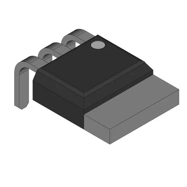
Infineon Technologies SPI11N60S5

Infineon SPI11N60S5 CoolMOS N-Channel MOSFET, 600V, 11A

MPNSPI11N60S5
End of Life

Infineon CoolMOS™ SPI11N60S5, N-Channel MOSFET, 600V Vdss, 11A Id, 380mOhm Rds(on) @ 7A, 10V, 54nC Qg, TO-262-3 (PG-TO262-3-1) package, Through Hole, -55°C to 150°C.

$1.07Ref. price · indicative, final on quote
PackagingTO-262-3 Long Leads, I²Pak, TO-262AA
StockContact for availability
MOQ1 pcs
  • 100% new & originalTraceable channels only — no refurbs, no pulls, no remarked parts.
  • Date & lot codes on quoteStated per line before you commit; label photos on request.
  • MSL-compliant ESD packingMoisture-sealed bags with indicator cards; reels photo-verified.
  • PayPal buyer protectionPay by T/T, PayPal or Payoneer — card payments covered end to end.

Specifications

SPI11N60S5 Technical Specifications
ParameterValue
SeriesCoolMOS™
FET typeN-Channel
Mounting typeThrough Hole
Drain to source voltage600 V
Drive voltage (Max rds on, min rds on)10V
Current - continuous drain (Id) @ 25°C11A (Tc)
Power dissipation125W (Tc)
Operating temperature-55°C ~ 150°C (TJ)
PackageBulk
Vgs±20V
TechnologyMOSFET (Metal Oxide)
CaseTO-262-3 Long Leads, I²Pak, TO-262AA
Vgs(th) (Max) @ id5.5V @ 500µA
Rds on (Max) @ id, vgs380mOhm @ 7A, 10V
Gate charge (Qg) (Max) @ vgs54 nC @ 10 V
Input capacitance (Ciss) (Max) @ vds1460 pF @ 25 V

Product details

600V CoolMOS N-channel — switching power supply workhorse

The through-hole TO-262 (I²Pak) package with long leads allows the backside tab to be bolted to a heatsink, pulling heat into the chassis rather than the board.

The 54 nC total gate charge at 10 V is moderate for a 600 V, 11 A device — a gate driver with 1 A peak source/sink capability can switch it in the 50–100 ns range, keeping crossover losses manageable at 50–100 kHz. Input capacitance Ciss is 1460 pF at 25 V drain-source, which sets the gate-drive impedance required to avoid Miller-plateau ringing. The 125 W power dissipation ceiling in the TO-262 package means the thermal interface to the heatsink is the real limit on continuous output current, not the die itself.

For a production BOM, this means no near-term requalification risk.

Temperature range and thermal design boundary

The 125 W power dissipation figure at Tc=25°C is the theoretical maximum with an infinite heatsink; real-world designs derate based on the thermal resistance of the TO-262 tab-to-heatsink interface and the ambient air temperature inside the enclosure.

Frequently asked questions

What is the Rds(on) of the SPI11N60S5?

This is the conduction-loss figure used for efficiency calculations in the target SMPS application.