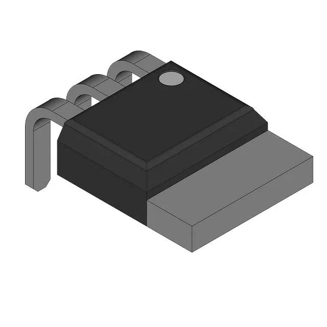
Infineon Technologies SPI07N65C3XKSA1

Infineon SPI07N65C3XKSA1 CoolMOS™ N-Channel MOSFET, 650 V

MPNSPI07N65C3XKSA1
End of Life

Infineon CoolMOS™ series SPI07N65C3XKSA1, N-Channel MOSFET, 650 V Vdss, 7.3 A Id, 600 mOhm Rds(on) @ 10 V, TO-262-3 (PG-TO262-3-1) through-hole package, -55°C to 150°C operating junction temperature.

$0.83Ref. price · indicative, final on quote
PackagingTO-262-3 Long Leads, I²Pak, TO-262AA
StockContact for availability
MOQ1 pcs
  • 100% new & originalTraceable channels only — no refurbs, no pulls, no remarked parts.
  • Date & lot codes on quoteStated per line before you commit; label photos on request.
  • MSL-compliant ESD packingMoisture-sealed bags with indicator cards; reels photo-verified.
  • PayPal buyer protectionPay by T/T, PayPal or Payoneer — card payments covered end to end.

Specifications

SPI07N65C3XKSA1 Technical Specifications
ParameterValue
SeriesCoolMOS™
FET typeN-Channel
Mounting typeThrough Hole
Drain to source voltage650 V
Drive voltage (Max rds on, min rds on)10V
Current - continuous drain (Id) @ 25°C7.3A (Tc)
Power dissipation83W (Tc)
Operating temperature-55°C ~ 150°C (TJ)
PackageBulk
Vgs±20V
TechnologyMOSFET (Metal Oxide)
CaseTO-262-3 Long Leads, I²Pak, TO-262AA
Vgs(th) (Max) @ id3.9V @ 350µA
Rds on (Max) @ id, vgs600mOhm @ 4.6A, 10V
Gate charge (Qg) (Max) @ vgs27 nC @ 10 V
Input capacitance (Ciss) (Max) @ vds790 pF @ 25 V

Product details

650 V CoolMOS™ — what the ratings mean for the switching stage

The Infineon SPI07N65C3XKSA1 is an N-channel power MOSFET from the CoolMOS™ series. Rated at 650 V drain-to-source and 7.3 A continuous drain current at 25°C case temperature, it targets the primary switching stage of offline AC-DC converters, power-factor-correction (PFC) boost stages, and flyback topologies. The 600 mOhm maximum on-resistance at 10 V gate drive sets the conduction loss budget; with 27 nC typical gate charge, the driver sees a light capacitive load. The TO-262-3 (PG-TO262-3-1) through-hole package suits wave-soldered boards where a heatsink can be bolted to the tab.

Gate-drive and switching behaviour

The 10 V gate-drive level for the rated Rds(on) is standard for CoolMOS™; the ±20 V absolute maximum gate-source voltage gives headroom for ringing on a hard-switched node. The 790 pF input capacitance at 25 V drain bias translates to a moderate switching loss. For soft-switching topologies (LLC, phase-shifted full bridge) the 27 nC gate charge keeps the circulating energy manageable.

Thermal budget and mounting

The 83 W maximum power dissipation at case temperature assumes a heatsink held at 25°C — in practice, the junction-to-case thermal path through the TO-262 tab needs a properly greased or pad-insulated heatsink. The -55°C to 150°C junction temperature range covers cold-start in outdoor telecom cabinets and full-load thermal cycling in enclosed power supplies. The through-hole mounting (PG-TO262-3-1) is a three-lead I²Pak-compatible footprint; the centre drain tab is the primary heat path, so the PCB copper area under the tab matters less than the heatsink interface.

Frequently asked questions

What is the Rds(on) of SPI07N65C3XKSA1?

The maximum on-resistance is 600 mOhm at a drain current of 4.6 A with a 10 V gate drive.

Is SPI07N65C3XKSA1 RoHS compliant?

Yes, it is ROHS3 compliant per Infineon's classification.

Is SPI07N65C3XKSA1 equivalent to FQA7N65?

Both are 650 V N-channel MOSFETs in similar through-hole packages, but the FQA7N65 has a different gate-threshold voltage and package marking. Verify the gate-drive circuit and pad layout before substituting — the CoolMOS™ C3 technology also gives a different switching characteristic (lower gate charge, faster body diode recovery) that may affect EMI or dead-time timing.