Gate drive and switching parasitics
The 4.5 V drive voltage for minimum Rds(on) means it can run from a 5 V logic-level gate signal, though the full 10 V drive delivers the rated 6.4 mOhm. The ±20 V Vgs max gives headroom for gate-drive overshoot in hard-switching topologies.
Thermal budget and package
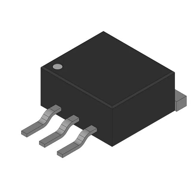
Maximum power dissipation is 136 W at the case, but the junction-to-ambient thermal path through the PG-TO252 (DPak) surface-mount package limits practical continuous dissipation on a standard PCB.