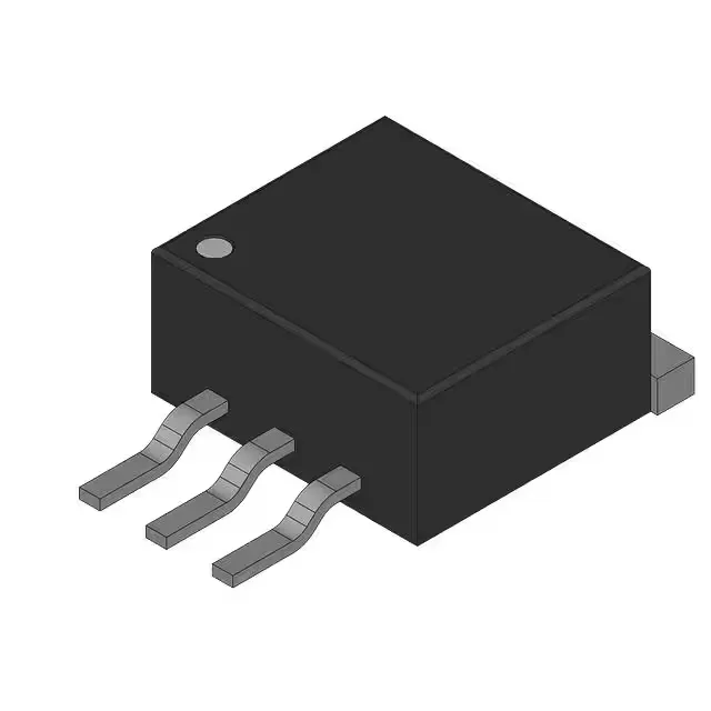
Infineon Technologies SPD03N60S5

Infineon SPD03N60S5 CoolMOS N-Ch MOSFET, 600V, 3.2A, TO-252

MPNSPD03N60S5
End of Life

Infineon CoolMOS™ SPD03N60S5, N-Channel Power MOSFET, 600 V Vdss, 3.2 A Id, 1.4 Ohm Rds(on) at 2 A, 10 V, 16 nC gate charge, TO-252-3 (DPak) package, -55 to 150 °C junction temperature, ROHS3 compliant.

$0.49Ref. price · indicative, final on quote
PackagingTO-252-3, DPak (2 Leads + Tab), SC-63
StockContact for availability
MOQ1 pcs
  • 100% new & originalTraceable channels only — no refurbs, no pulls, no remarked parts.
  • Date & lot codes on quoteStated per line before you commit; label photos on request.
  • MSL-compliant ESD packingMoisture-sealed bags with indicator cards; reels photo-verified.
  • PayPal buyer protectionPay by T/T, PayPal or Payoneer — card payments covered end to end.

Specifications

SPD03N60S5 Technical Specifications
ParameterValue
SeriesCoolMOS™
FET typeN-Channel
Mounting typeSurface Mount
Drain to source voltage600 V
Drive voltage (Max rds on, min rds on)10V
Current - continuous drain (Id) @ 25°C3.2A (Tc)
Power dissipation38W (Tc)
Operating temperature-55°C ~ 150°C (TJ)
PackageBulk
Vgs±20V
TechnologyMOSFET (Metal Oxide)
CaseTO-252-3, DPak (2 Leads + Tab), SC-63
Vgs(th) (Max) @ id5.5V @ 135µA
Rds on (Max) @ id, vgs1.4Ohm @ 2A, 10V
Gate charge (Qg) (Max) @ vgs16 nC @ 10 V
Input capacitance (Ciss) (Max) @ vds420 pF @ 25 V

Product details

600 V CoolMOS™ N-channel — what it brings to the switching stage

The Infineon SPD03N60S5 is a 600 V N-channel CoolMOS™ power MOSFET in a TO-252-3 (DPak) surface-mount package. It is rated for 3.2 A continuous drain current at 25 °C case temperature and carries a 1.4 Ohm maximum on-resistance when driven with a 10 V gate signal. The 16 nC typical gate charge keeps switching losses manageable in hard-switched topologies like PFC boost stages, flyback converters, and auxiliary power supplies. Junction temperature spans -55 to 150 °C, so it handles the thermal cycling of outdoor telecom or industrial power supplies without derating at the cold end.

Package and mounting — TO-252-3 (DPak) land pattern

The SPD03N60S5 uses the standard TO-252-3 (DPak) footprint with a single drain tab. The supplier device code is PG-TO252-3-313. The tab is the drain terminal; ensure the PCB copper area under the tab is sized for heat spreading — the 38 W dissipation rating assumes adequate board-level thermal management. No heatsink is needed at moderate loads, but a thermal pad or via array under the tab helps keep the junction below 150 °C in continuous operation.

Lifecycle and compliance — active, no LTB watch

Infineon lists the SPD03N60S5 as Active with no end-of-life notification. ROHS3 compliance is confirmed, so it passes EU material restrictions for new designs. The CoolMOS™ S5 series is a mature, still-shipping portfolio; no second-source or direct replacement is needed for supply continuity. For BOM-freeze planning, this part carries no imminent PCN risk.

Frequently asked questions

What is the Rds(on) of SPD03N60S5?

Maximum on-resistance is 1.4 Ohm at 2 A drain current with a 10 V gate drive.

Is SPD03N60S5 compatible with IRF830?

Both are 500 V / 600 V class N-channel MOSFETs, but the SPD03N60S5 is a surface-mount TO-252 part while the IRF830 is a through-hole TO-220. Footprint and thermal management differ. The SPD03N60S5 has lower gate charge (16 nC vs roughly 30 nC for IRF830) and a higher voltage rating (600 V vs 500 V). They are not pin-compatible; a board redesign is needed to swap.

What is the closest pin-compatible alternative to SPD03N60S5?

Within the CoolMOS™ S5 family, the SPD03N60S5 has no direct pin-compatible sibling with identical ratings. For a drop-in replacement in the same TO-252 footprint, consider the SPD04N60S5 (4 A, lower Rds(on)) if the current margin allows. Verify gate charge and switching behaviour against the circuit.