600 V CoolMOS in a TO-263 — what this part does
The SPB02N60C3: The 600 V drain-to-source rating (Vdss) places it in the high-voltage switching tier — suitable for flyback converters, PFC stages, and auxiliary power supplies where the bulk rail sits at 400 VDC or below.
Switching losses and thermal budget
The 200 pF input capacitance at 25 V drain-source is a direct measure of the gate-drive load at turn-on. Paired with the 12.5 nC gate charge, the switching energy per cycle is low enough that a 25 W maximum power dissipation (Tc) is the practical ceiling — the designer sizes the heatsink to keep the junction below 150 °C under worst-case load. Gate threshold voltage is specified at 3.9 V maximum at 80 µA drain current, which means a 10 V drive rail (the recommended drive voltage for minimum Rds(on)) gives ample overdrive margin. The ±20 V absolute maximum gate-source rating leaves headroom for ringing on the gate node in a hard-switched topology.
Package and board integration
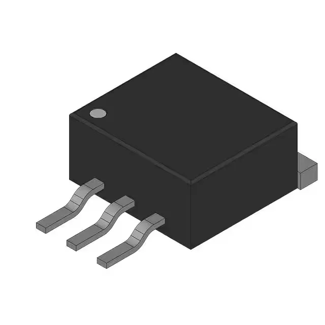
The SPB02N60C3 is supplied in a TO-263-3 (D²Pak) surface-mount package, supplier code PG-TO263-3-2. The large exposed drain tab on the bottom provides a low thermal resistance path to the PCB copper plane — the board layout must allocate enough copper area on the drain pad to dissipate the 25 W maximum. The three-lead footprint is standard for D²Pak; the centre lead is the drain, the outer two are source and gate.
