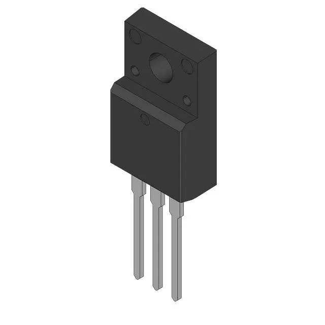
Obsolete — sourcing the SPA21N50C3XKSA1 today
The 560 V drain-source breakdown voltage (Vdss) places this MOSFET in the 500–600 V class, suitable for offline flyback converters, PFC stages, and high-voltage DC-DC converters where the bus voltage can reach 400 VDC with margin for transients. Continuous drain current is rated 21 A at 25 °C case temperature (Tc), but the 34.5 W power dissipation ceiling in the TO-220 Full Pack package means the practical current at elevated ambient drops quickly — derate for the junction temperature limit of 150 °C. At 25 °C junction this is the conduction-loss floor; at 125 °C junction the on-resistance roughly doubles, so budget 380 mOhm for worst-case thermal design.
Gate drive and switching considerations
Total gate charge (Qg) is 95 nC at 10 V gate voltage. Input capacitance (Ciss) is 2400 pF at 25 V drain-source. This moderate capacitance keeps the switching losses manageable in hard-switched topologies, but the driver output impedance should be low enough to charge Ciss within the desired dead-time window. Gate-source voltage is limited to ±20 V maximum.
This simplifies assembly but increases thermal resistance compared to a standard TO-220 with a bare tab. In practice, the junction-to-case thermal resistance limits the heat that can be extracted; a forced-air heatsink or larger thermal mass is needed to stay below 150 °C junction at high load. The full temperature range is useful for avionics, downhole, or outdoor telecom equipment where ambient can swing widely.