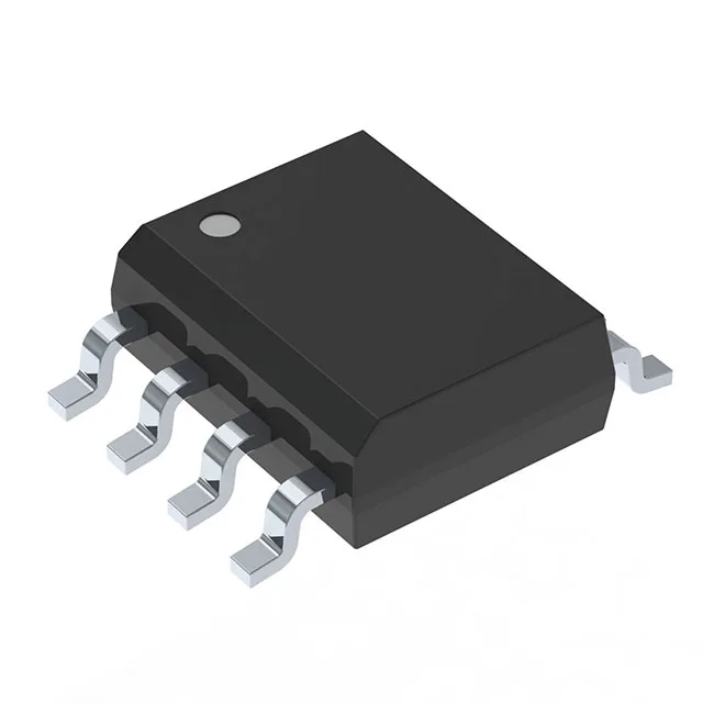
30 V, 9 mΩ, 12.5 A — where this HEXFET fits
This combination targets low-voltage, high-current switching applications: synchronous rectification in 12 V input DC-DC converters, load switches, and OR-ing circuits where the 30 V Vdss provides margin for 12 V bus transients.
For a new design, the official recommendation is to select a current-production N-channel MOSFET with similar 30 V / 9 mΩ / 12.5 A ratings in an SO-8 footprint. For an existing BOM that already uses this part, the supply channel shifts to independent distribution — surplus stock, last-time-buy inventory, and broker-sourced material. Sourcing through this channel is feasible but requires qualification of date codes and verification against counterfeit risk, especially for high-reliability or safety-critical builds.
Key ratings for the switching design
The 30 V drain-to-source rating gives enough headroom for a nominal 12 V rail with ringing clamped to 24 V, but not for a 24 V system — that needs a 40 V or 60 V device. The 4.5 V drive voltage option allows logic-level gate drive from a 5 V or 3.3 V GPIO, but the Rds(on) at 4.5 V is not specified — expect it to be higher than the 9 mΩ at 10 V, so verify against the datasheet curve if using reduced gate drive. Input capacitance of 2240 pF at 15 V is moderate; switching at 200–500 kHz is practical with a standard gate driver.
The 150°C rating is the junction limit — the case temperature will be lower, and the 2.5 W dissipation at 25°C ambient must be derated above 25°C per the thermal derating curve in the datasheet.