SiC Schottky — zero recovery loss in the PFC boost stage
In a PFC boost stage, this part replaces a silicon ultrafast diode and cuts diode-related switching loss.
Forward voltage and junction temperature — thermal design anchors
That 8.5 W conduction loss at full rated current sets the thermal budget: with a junction-to-case thermal resistance typical of a TO-220, the designer needs a heatsink sized to keep Tj below 175 °C. The 170 pF capacitance at 1 V reverse bias keeps capacitive switching losses manageable at high frequencies.
Package and mounting — through-hole with a tab cathode
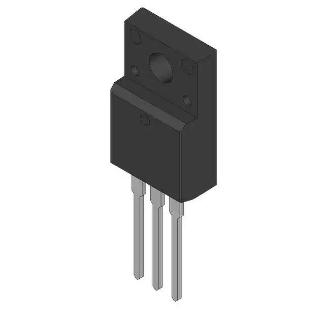
Housed in a PG-TO220-2, this is a two-lead through-hole package with the metal tab forming the cathode connection. The tab must be electrically isolated from the heatsink or tied to the output rail, depending on the topology. The through-hole body is straightforward to hand-solder and rework, which matters for prototype builds and low-to-medium volume production.