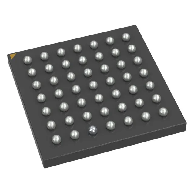
Infineon Technologies S80KS2564GACHI040 — Analog & Data Acquisition

Infineon S80KS2564GACHI040 HYPERRAM™ 256 Mbit PSRAM, 200 MHz

MPNS80KS2564GACHI040
End of Life

Infineon HYPERRAM™ S80KS2564GACHI040, 256 Mbit PSRAM, HyperBus interface, 35 ns access time, 200 MHz clock, 1.7V–2V supply, 49-FBGA (8x8), -40°C to 85°C.

$15.55Ref. price · indicative, final on quote
Packaging49-VBGA
StockContact for availability
MOQ1 pcs
  • 100% new & originalTraceable channels only — no refurbs, no pulls, no remarked parts.
  • Date & lot codes on quoteStated per line before you commit; label photos on request.
  • MSL-compliant ESD packingMoisture-sealed bags with indicator cards; reels photo-verified.
  • PayPal buyer protectionPay by T/T, PayPal or Payoneer — card payments covered end to end.

Specifications

S80KS2564GACHI040 Technical Specifications
ParameterValue
SeriesHYPERRAM™
Memory typeVolatile
Mounting typeSurface Mount
Voltage1.7V ~ 2V
Frequency200 MHz
Memory interfaceHyperBus
Operating temperature-40°C ~ 85°C (TA)
PackageTray
TechnologyPSRAM (Pseudo SRAM)
Access time35 ns
Memory size256Mbit
Memory formatPSRAM
Case49-VBGA
Memory organization16M x 16
Write cycle time - word, page35ns

Product details

256 Mbit HYPERRAM™ — dense volatile storage on a narrow bus

Infineon's S80KS2564GACHI040 is a 256 Mbit Pseudo SRAM (PSRAM) from the HYPERRAM™ series, designed as a pin-efficient volatile memory expansion for SoCs with a HyperBus controller. It combines the density of DRAM with an SRAM-like interface, eliminating the need for refresh management from the host. The part runs on a 1.7 V to 2 V supply and communicates over a HyperBus at up to 200 MHz, delivering a 35 ns initial access time and sustained throughput suitable for code shadowing, display frame buffers, or packet buffering in embedded systems.

35 ns access time — what it means for the bus

The 35 ns access time is the random-read latency from the first HyperBus command to the first data word. In a system with a 200 MHz HyperBus clock (5 ns period), this translates to about 7 clock cycles before data starts streaming. This is on par with other HYPERRAM devices and well within the timing budget for most Cortex-M and RISC-V SoCs that integrate a HyperBus controller. The 200 MHz clock also gives a theoretical peak data rate of 400 MB/s in DDR mode (double data rate), though real throughput depends on controller efficiency and bus utilization.

Industrial temperature and supply range

Rated for -40°C to 85°C ambient, this part is suited for outdoor telecom, factory automation, and industrial control enclosures where temperature swings are common. The 1.7 V to 2 V supply range aligns with low-power SoC rails; note the upper limit is 2 V, not the typical 3.3 V, so a dedicated regulator or PMIC rail is required. The 49-FBGA (8x8 mm) package uses a 0.8 mm ball pitch, which is routable on a standard 4-layer PCB with blind vias if needed.

Active lifecycle — no LTB risk

S80KS2564GACHI040 carries an Active lifecycle status. It is ROHS3 compliant. For new designs, this part is a safe selection today, though as with any single-sourced memory, maintaining a qualified second source is good practice for production continuity.

Frequently asked questions

What is the access time of S80KS2564GACHI040?

The S80KS2564GACHI040 has a 35 ns initial access time for random reads on the HyperBus interface.

Is S80KS2564GACHI040 active or obsolete?

It is Active per the manufacturer's lifecycle status — no discontinuation or last-time-buy is in effect.

What is the difference between HyperRAM and HyperFlash?

HyperRAM (like this S80KS2564GACHI040) is volatile PSRAM used for temporary data storage, while HyperFlash is non-volatile NOR Flash for code storage. Both use the same HyperBus interface, but HyperFlash has longer access times (e.g., 96 ns for the S26KS128SDPBHV020) and is not a functional replacement.

Is S80KS2564GACHI040 compatible with SoCs supporting HyperBus?

Yes, any SoC with a HyperBus controller operating at 1.7 V to 2 V and supporting a 200 MHz clock can interface directly with this part. The HyperBus protocol is standardized, so no glue logic is needed.