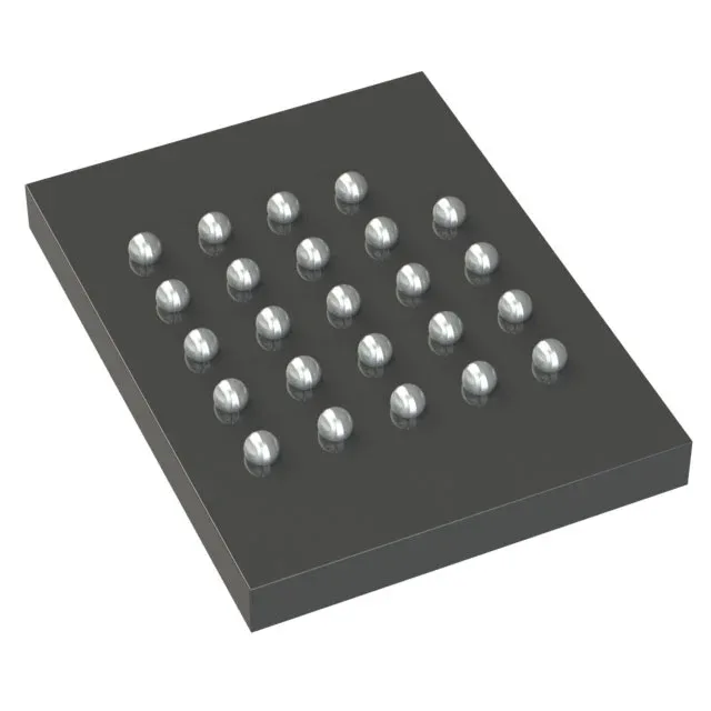
Infineon Technologies S80KS2563GABHB020 — Analog & Data Acquisition

Infineon S80KS2563GABHB020 HYPERRAM 256Mbit PSRAM

MPNS80KS2563GABHB020
End of Life

Infineon HYPERRAM series, S80KS2563GABHB020, 256Mbit PSRAM, Octal SPI interface, 200 MHz clock, 35 ns access, 1.7V-2V supply, -40°C to 105°C, 24-FBGA (6x8) package, Tray.

$13.57Ref. price · indicative, final on quote
Packaging24-VBGA
StockContact for availability
MOQ1 pcs
  • 100% new & originalTraceable channels only — no refurbs, no pulls, no remarked parts.
  • Date & lot codes on quoteStated per line before you commit; label photos on request.
  • MSL-compliant ESD packingMoisture-sealed bags with indicator cards; reels photo-verified.
  • PayPal buyer protectionPay by T/T, PayPal or Payoneer — card payments covered end to end.

Specifications

S80KS2563GABHB020 Technical Specifications
ParameterValue
SeriesHYPERRAM™
Memory typeVolatile
Mounting typeSurface Mount
Voltage1.7V ~ 2V
Frequency200 MHz
Memory interfaceSPI - Octal I/O
Operating temperature-40°C ~ 105°C (TA)
PackageTray
TechnologyPSRAM (Pseudo SRAM)
Access time35 ns
Memory size256Mbit
Memory formatPSRAM
Case24-VBGA
Memory organization32M x 8
Write cycle time - word, page35ns

Product details

256 Mbit PSRAM with Octal SPI — what it is and where it fits

The Infineon S80KS2563GABHB020 is a 256 Mbit Pseudo SRAM (PSRAM) from the HYPERRAM family, designed to deliver high-density volatile storage through a low-pin-count Octal SPI interface. It is organized as 32M x 8 bits and operates from a 1.7V to 2V supply, making it a natural fit for 1.8V system rails without additional level translation. The part is targeted at applications that need a large scratchpad, display frame buffer, or code-shadowing memory where the simplicity of a serial interface and the density of a DRAM-like cell (managed internally as PSRAM) beat the cost or board area of a true SRAM.

200 MHz Octal I/O and 35 ns access — what they mean for throughput

The Octal SPI interface runs at 200 MHz, delivering a theoretical peak data rate of 200 MB/s (200 MHz x 8 bits per cycle). The 35 ns access time covers the initial random-access latency; once the device is in page mode, subsequent reads within the same row run at the full clock rate. For a design currently using a Quad SPI Flash for code execution and needing a separate RAM for dynamic data, this part can often share the same bus with a chip-select mux, simplifying layout. The 35 ns write cycle time per word or page matches the read access, so mixed read-write workloads see symmetric latency.

Temperature grade and environment

Rated for -40°C to 105°C ambient, this part covers industrial and extended-temperature applications: outdoor telecom, motor drives, engine bay electronics, and factory-floor controllers. The 24-ball FBGA (6x8 mm) package is a fine-pitch BGA that requires controlled-depth vias and a clean PCB stack-up for signal integrity at 200 MHz.

Lifecycle and sourcing posture

The S80KS2563GABHB020 carries an Active product status with ROHS3 compliance.

Frequently asked questions

Where can I buy S80KS2563GABHB020?

The S80KS2563GABHB020 is sourced through independent distribution and quoted to order against an RFQ. Availability and current pricing are confirmed at the time of quote — submit an RFQ through this listing.

Is S80KS2563GABHB020 compatible with 1.8V systems?

Yes. The supply voltage range is 1.7V to 2V, which covers the standard 1.8V system rail directly. The Octal I/O pins operate at the same VDDQ level, so no external level shifters are needed for a 1.8V memory bus.