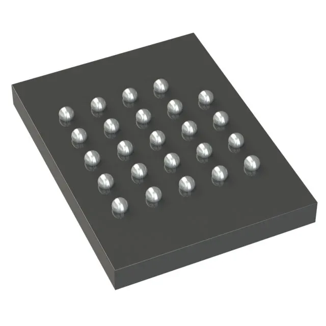
256 Mbit Flash + 64 Mbit RAM in a single 24-FBGA package
The Cypress S71KL256SC0BHB000 is a multi-chip package memory device from the Automotive AEC-Q100 HyperFlash™ + HyperRAM™ KL series, integrating 256 Mbit of non-volatile Flash and 64 Mbit of volatile DRAM on a shared parallel bus. This die-stack approach eliminates the need for separate Flash and RAM ICs, saving PCB area and reducing interconnect complexity in space-constrained automotive ECUs.
The parallel memory interface runs at 100 MHz, providing sufficient bandwidth for code shadowing, real-time data logging, and display frame buffering in automotive infotainment and instrument cluster applications. Because both the Flash and RAM share the same bus, the host MCU or SoC can execute code directly from the HyperFlash while using the HyperRAM for scratchpad or temporary storage without additional chip selects or address decoding. The 256 Mbit Flash density supports firmware images with over-the-air update staging, while the 64 Mbit RAM handles moderate-sized data buffers without external SRAM.
Package and footprint — 24-FBGA (6x8 mm)
Housed in a 24-ball VBGA package measuring 6x8 mm (24-FBGA), this part is designed for surface-mount assembly. The BGA footprint requires careful PCB layout for signal integrity at 100 MHz — keep the parallel bus traces length-matched and provide solid decoupling between the 2.7 V and 3.6 V supply rails. The compact size suits multi-layer automotive PCBs where every square millimeter counts.
It is ROHS3 compliant.