1 Gbit NOR Flash for code shadowing and data logging
66 MHz Quad I/O — read throughput for the boot path
Quad I/O at 66 MHz delivers an effective read throughput of 33 MB/s in single-data-rate mode — enough for direct code execution (XIP) from the Flash in most MCU-based designs. The 2.7 V supply rail is compatible with 3.3 V SPI buses; the input thresholds are VCC-referenced, so a 3.3 V host driving the S70FL01GSDPMFV010 at 2.7 V VCC sees a valid logic-high as long as the host output meets VIH(min) of 0.7 × VCC (1.89 V).
For dual-sourcing resilience, the 512 Mbit sibling S25FL512SAGBHV210 shares the same FL-S family and Quad I/O interface but at half the density and a faster 133 MHz clock — it is a functional alternative only if the firmware fits in 512 Mbit.
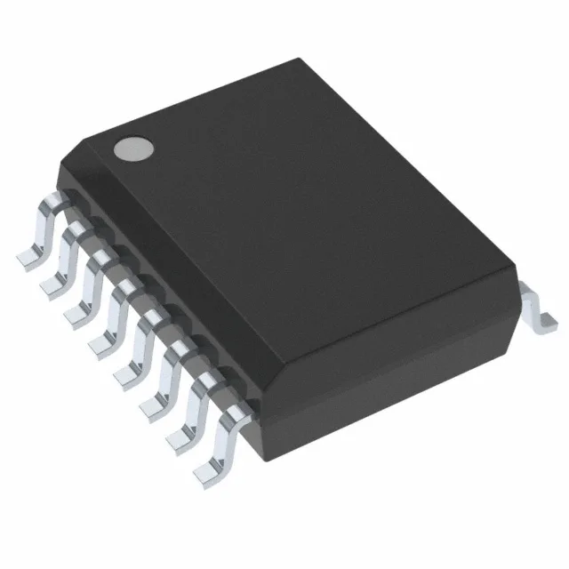
Package and footprint — 16-SOIC
The SPI Quad I/O signals (CS#, SCK, SI/SIO0, SO/SIO1, WP#/SIO2, HOLD#/SIO3) occupy six pins, leaving the rest for supply and no-connects. The package is rated for surface-mount assembly and ships in tray form.