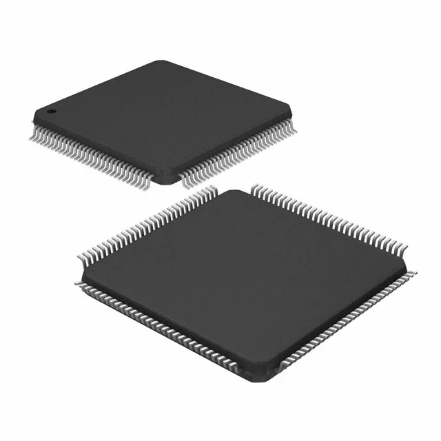
The S6E2HE6G0AGV20000: Program memory is 544 KB of on-chip Flash, with 64 K × 8 SRAM for data and stack. That Flash density holds a full communication stack (EtherCAT or CANopen) plus application code without external memory. The 100 GPIO pins, mapped through a 120-LQFP (16×16 mm) package, give enough headroom for parallel EBI/EMI buses, SD card interfaces, and a bank of I²C or UART peripherals simultaneously.
Temperature grade and supply — industrial and automotive environments
On-chip data converters include a 24-channel 12-bit ADC and a dual 12-bit DAC. The dual DAC can generate analog setpoints or reference voltages for external analog circuits.
Peripherals and connectivity — what is on the bus
Peripheral set includes DMA, LVD (low-voltage detect), POR (power-on reset), PWM timers, and a watchdog timer. Connectivity covers CSIO (clocked serial I/O), EBI/EMI (external bus interface for parallel memory or FPGA), I²C, LINbus, SD card interface, and UART/USART.