Infineon Technologies S6E2C4AJ0AGB1000A — Sensors & Transducers

S6E2C4AJ0AGB1000A Infineon MCU – 200 MHz Cortex-M4F

MPNS6E2C4AJ0AGB1000A
End of Life

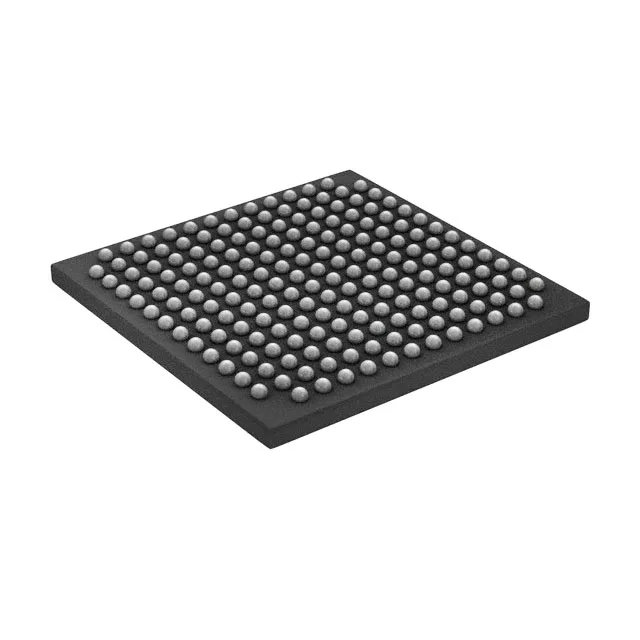
Infineon Technologies FM4 S6E2C4 series, S6E2C4AJ0AGB1000A, ARM Cortex-M4F 32-bit MCU, 200 MHz, 2 MB Flash, 256 KB SRAM, 152 I/O, 192-FBGA (12x12 mm), -40°C to 125°C, Active.

$21.23Ref. price · indicative, final on quote
Packaging192-LFBGA
StockContact for availability
MOQ1 pcs
  • 100% new & originalTraceable channels only — no refurbs, no pulls, no remarked parts.
  • Date & lot codes on quoteStated per line before you commit; label photos on request.
  • MSL-compliant ESD packingMoisture-sealed bags with indicator cards; reels photo-verified.
  • PayPal buyer protectionPay by T/T, PayPal or Payoneer — card payments covered end to end.

Specifications

S6E2C4AJ0AGB1000A Technical Specifications
ParameterValue
SeriesFM4 S6E2C4
Mounting typeSurface Mount
Oscillator typeInternal
Program memory typeFLASH
Voltage - supply (Vcc (Vdd))2.7V ~ 5.5V
Operating temperature-40°C ~ 125°C (TA)
Speed200MHz
PackageTray
RAM size256K x 8
Core size32-Bit Single-Core
PeripheralsDMA, I²S, LVD, POR, PWM, WDT
ConnectivityCANbus, CSIO, EBI/EMI, I²C, LINbus, SD, SPI, UART/USART
Number of i (O)152
Core processorARM® Cortex®-M4F
Case192-LFBGA
Data convertersA/D 32x12b; D/A 2x12b
Program memory size2MB (2M x 8)

Product details

200 MHz Cortex-M4F with 2 MB Flash — headroom for sensor fusion and motor control

The S6E2C4AJ0AGB1000A is an Infineon FM4 series MCU built around an ARM Cortex-M4F core running at 200 MHz. That clock rate, combined with a single-cycle multiply-accumulate and floating-point unit, gives it the throughput to handle sensor fusion algorithms, FOC motor control loops, and real-time Ethernet stacks without an external DSP. Program memory is 2 MB of on-chip Flash, backed by 256 KB SRAM — enough to hold a full RTOS, application code, and a data-logging buffer for predictive maintenance logs.

152 I/O and wide supply range — BOM-fit for mixed-voltage systems

With 152 general-purpose I/O lines, this MCU can interface directly to parallel LCDs, external memory buses (EBI/EMI), and multiple CAN or SPI peripherals without a port expander.

Active production — no end-of-life risk for new designs

For volume commitments, pricing and lead time are confirmed per RFQ against your BOM quantity.

192-FBGA (12x12 mm) — compact footprint, 4+ layer PCB recommended

The 192-ball FBGA package measures 12x12 mm with a 0.50 mm ball pitch. Fan-out of the inner rows requires at least a 4-layer PCB with microvias or blind vias; a 2-layer board will only break out the perimeter balls. The small footprint is an advantage in space-constrained designs like handheld instruments or compact drives.

Frequently asked questions

What is the closest functional second-source for the S6E2C4AJ0AGB1000A?

It is not a pin-compatible drop-in — the package and peripheral set differ. For a closer match within the Infineon portfolio, the XMC4200F64F256BAXQMA1 (XMC4000 series, Cortex-M4 at 80 MHz) offers similar data converters but only 35 I/O and a smaller Flash footprint.