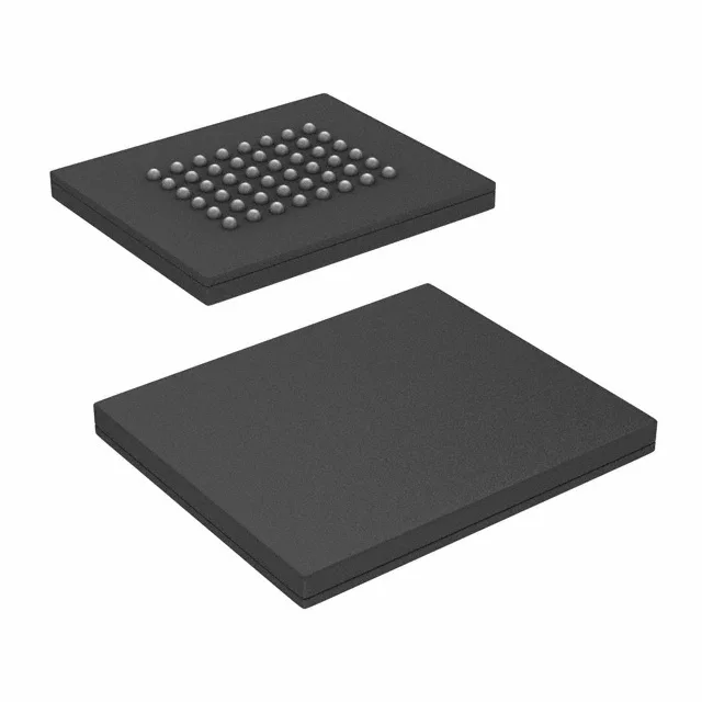
64 Mbit parallel NOR Flash in a 48-ball BGA
The Infineon (Cypress) S29JL064J55BHI003 is a 64 Mbit parallel NOR Flash memory from the JL-J series, organized as 8M x 8 or 4M x 16 bits.
The 55 ns access time means the memory can return data within 55 ns of the address being valid. For a 48 MHz MCU with a 20.8 ns clock period, this allows zero-wait-state reads with a little margin; at 72 MHz (13.9 ns period), the bus controller will insert one wait state. The page-mode write cycle time is also 55 ns, so back-to-back writes to the same page run at full speed. If your design currently uses a 70 ns or 90 ns parallel NOR part, this 55 ns device gives you headroom for a faster bus clock or tighter timing closure.
FBGA footprint — plan the reflow profile
The 48-VFBGA package (8.15 x 6.15 mm body) uses a fine-pitch ball array. This is a surface-mount BGA, so the board needs solder mask defined pads, X-ray inspection after reflow, and a controlled reflow profile per the moisture sensitivity level. The supplier device package is 48-FBGA (8.15x6.15). Store the reels dry — MSL level is not stated in this listing, but assume MSL 3 unless confirmed otherwise. If the dry-pack has been open, bake before reflow.
ROHS3 compliance is confirmed. The S25FL064LABNFI043 is a 64 Mbit SPI NOR, which uses a serial interface and is not pin-compatible.