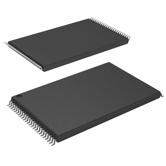
Infineon Technologies S29JL032J70TFI410 — Discrete Semiconductors

Infineon S29JL032J70TFI410 32Mbit NOR Flash, 70ns, 48-TSOP

MPNS29JL032J70TFI410
End of Life

Infineon Technologies JL-J series NOR Flash memory, S29JL032J70TFI410, 32Mbit, 70 ns access time, 2.7-3.6 V, Parallel interface, 48-TSOP, Tray.

$5.09Ref. price · indicative, final on quote
Packaging48-TFSOP (0.724", 18.40mm Width)
StockContact for availability
Lead timeIn Stock wk
MOQ1 pcs
  • 100% new & originalTraceable channels only — no refurbs, no pulls, no remarked parts.
  • Date & lot codes on quoteStated per line before you commit; label photos on request.
  • MSL-compliant ESD packingMoisture-sealed bags with indicator cards; reels photo-verified.
  • PayPal buyer protectionPay by T/T, PayPal or Payoneer — card payments covered end to end.

Specifications

S29JL032J70TFI410 Technical Specifications
ParameterValue
SeriesJL-J
Memory typeNon-Volatile
Mounting typeSurface Mount
Voltage2.7V ~ 3.6V
Memory interfaceParallel
Operating temperature-40°C ~ 85°C (TA)
PackageTray
TechnologyFLASH - NOR
Access time70 ns
Memory size32Mbit
Memory formatFLASH
Case48-TFSOP (0.724\", 18.40mm Width)
Memory organization4M x 8, 2M x 16
Write cycle time - word, page70ns

Product details

70 ns read access defines the code-execution ceiling

The S29JL032J70TFI410 is a 32 Mbit parallel NOR flash from Infineon's JL-J series, organized as 4M x 8 or 2M x 16 bits. The 70 ns access time sets the random-read latency — the time from address assertion to valid data on the bus — which directly limits the CPU clock speed for execute-in-place (XIP) firmware. A 70 ns access at a 16-bit bus width yields roughly 28 MB/s sustained read throughput, adequate for boot code and parametric tables in embedded controllers. The parallel NOR interface eliminates the overhead of a serial protocol layer, giving deterministic read latency critical for real-time interrupt service routines and boot vector fetch. The write cycle time per word or page matches the read access at 70 ns, so page-mode programming keeps the same bus timing.

Supply and temperature envelope for industrial embedded systems

The 48-TFSOP package (0.724" body width, 18.40 mm) uses a standard TSOP footprint with a 0.50 mm pin pitch. The 48-TSOP supplier device package variant shares the same land pattern — confirm the exact body thickness for the reflow profile, as TSOP packages are moisture-sensitive and require bake before reflow if exposed above the MSL floor life.

Active lifecycle and compliance baseline

For BOM risk mitigation, the JL-J series includes multiple density and speed grades sharing the same 48-TSOP footprint — a parametric search by package and supply voltage will identify drop-in alternatives within the same family.

Frequently asked questions

What is the memory organization and bus width of the S29JL032J70TFI410?

The 32 Mbit array is configurable as 4M x 8 bits or 2M x 16 bits, giving the designer a choice of 8-bit or 16-bit host bus interface without changing the package or pinout.

What compliance documentation does Infineon provide for the S29JL032J70TFI410?

The part is ROHS3 Compliant, covering all six original RoHS substances plus the four phthalates (DEHP, BBP, DBP, DIBP). Infineon typically provides a material declaration and REACH compliance statement upon request through the supply chain.