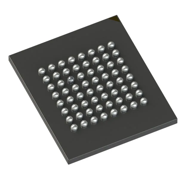
512 Mbit parallel NOR flash for code-shadowing and firmware storage
The S29GL512S11FHI010 is a 512 Mbit parallel NOR flash from Infineon's GL-S series, organized as 32M x 16 bits. The parallel interface delivers sustained read throughput for direct code execution (XIP) without the latency overhead of serial flash — a common requirement in boot-critical embedded systems where the CPU fetches instructions directly from the flash array. Access time is 110 ns, which sets the ceiling for random read latency from the memory bus. In a system with a 100 MHz controller, this translates to roughly 11 wait states per access — the system architect must budget this into the memory controller's timing configuration. Write cycle time (word/page) is 60 ns, relevant for firmware update windows where sector erase and program times dominate the total write budget.
Package footprint and rework considerations
Supplied in a 64-LBGA (11x13 mm FBGA) package on tray. The 0.8 mm ball pitch is standard for BGA rework — a hot-air reflow station with a preheat plate and a stencil for the bottom-side paste is sufficient. The package is moisture-sensitive; the tray format indicates the device ships in the moisture-barrier bag with a desiccant card. Bake at 125°C for 48 hours if the bag seal is broken or the humidity indicator card shows >10% RH before reflow.
Lifecycle status and compliance documentation
The GL-S series is Infineon's mainstream parallel NOR flash family, positioned between the legacy GL (non-ECC) and the newer GL-T (1.65 V core) variants. No pin-compatible second-source is officially cross-referenced by Infineon; the device is single-sourced from Infineon's own fabs. For volume BOMs, a risk-mitigation strategy is to qualify the GL-T sibling (S29GL512T11TFIV20) on the same board layout — but note the supply voltage difference: GL-T runs at 1.65 V core, requiring a separate regulator rail.