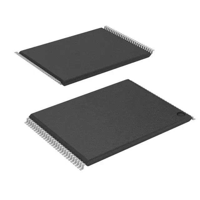
Infineon Technologies S29GL512S10TFI010 — Logic ICs

S29GL512S10TFI010 Cypress GL-S 512Mbit NOR Flash, 100 ns

MPNS29GL512S10TFI010
End of Life

Cypress GL-S series, S29GL512S10TFI010, 512Mbit Parallel NOR Flash, 100 ns access time, 2.7 V to 3.6 V supply, 32M x 16 organization, -40°C to 85°C, 56-TSOP package.

$9.26Ref. price · indicative, final on quote
Packaging56-TFSOP (0.724", 18.40mm Width)
RoHSRoHS non-compliant
SeriesGL-S
Independent supplier — new & surplus stockAuthenticity-screened · ESD-safe packingListing updated Aug 2026

Specifications

S29GL512S10TFI010 specifications
ParameterValue
SeriesGL-S
Memory typeNon-Volatile
MountingSurface Mount
Supply voltage2.7V ~ 3.6V
Memory interfaceParallel
Operating temperature-40°C ~ 85°C (TA)
PackageBulk
TechnologyFLASH - NOR
Access time100 ns
Memory size512Mbit
Memory formatFLASH
Case56-TFSOP (0.724\", 18.40mm Width)
Memory organization32M x 16
Write cycle time - word, page60ns

Product details

512 Mbit parallel NOR Flash for XIP and firmware storage

The Cypress S29GL512S10TFI010 is a 512 Mbit parallel NOR Flash memory from the GL-S family, organized as 32M x 16 bits. It uses a standard parallel interface for direct code execution (XIP) and firmware storage in embedded systems. The 100 ns access time is the speed grade that determines read-cycle timing with the host controller — at this density and voltage range, 100 ns is the baseline speed bin for the GL-S series.

100 ns access time and bus timing margin

In practice, this sets the fastest clock rate at which the host can read the Flash without wait states. Compared to the sibling S29GL512T11TFIV20 (110 ns access time, 1.65 V supply), this part offers a 10 ns faster access at the cost of a higher minimum supply voltage (2.7 V vs 1.65 V). The 60 ns write cycle time per word or page applies to program and erase operations — that timing is identical across the GL-S and GL-T families at this density.

56-TSOP footprint and board integration

The 56-TSOP package (0.724 inch body width, 18.40 mm) is a surface-mount form factor common for parallel NOR Flash in this density tier. The 32M x 16 organization maps directly to a 16-bit data bus — typical for ARM Cortex-M or PowerQUICC host processors that boot from external parallel Flash.

Frequently asked questions

What are the cross-reference or alternative parts for S29GL512S10TFI010?

The closest functional peer in the same density is the S29GL512T11TFIV20 (GL-T series), which offers a 110 ns access time and operates from 1.65 V supply — a lower-voltage option but with a slower read speed.

What is the memory organization of S29GL512S10TFI010?

The memory is organized as 32M words by 16 bits (32M x 16), giving a total of 512 Mbit. This 16-bit-wide organization connects directly to a 16-bit parallel data bus for efficient code execution.