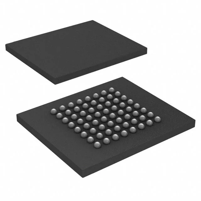
Infineon Technologies S29GL256S10FAIV20 — Memory (DRAM / SRAM / Flash / EEPROM)

S29GL256S10FAIV20 256 Mbit Parallel NOR Flash, 100 ns

MPNS29GL256S10FAIV20
Active

Infineon GL-S series S29GL256S10FAIV20, 256 Mbit Parallel NOR Flash, 100 ns access time, 2.7 V supply, 16M x 16 organization, 64-FBGA, -40°C to 85°C industrial temperature range.

$5.45Ref. price · indicative, final on quote
StockContact for availability
MOQ1 pcs
  • 100% new & originalTraceable channels only — no refurbs, no pulls, no remarked parts.
  • Date & lot codes on quoteStated per line before you commit; label photos on request.
  • MSL-compliant ESD packingMoisture-sealed bags with indicator cards; reels photo-verified.
  • PayPal buyer protectionPay by T/T, PayPal or Payoneer — card payments covered end to end.

Specifications

S29GL256S10FAIV20 Technical Specifications
ParameterValue
SeriesGL-S
Interface_typeParallel
Mounting_typeSurface Mount
Operating temperature high-40°C to 85°C (TA)
Frame_size256Mbit
Access time100 ns
Memory_typeNon-Volatile
Package_typeTray
Memory formatFLASH
Product_statusActive
Supply_voltage_v2.7
Memory organization16M x 16
Write cycle time - word, page60ns

Product details

256 Mbit parallel NOR Flash in a 64-FBGA footprint

The Infineon S29GL256S10FAIV20 is a 256 Mbit parallel NOR Flash memory from the GL-S series, organized as 16M x 16 bits. The 64-ball FBGA package saves board area compared to TSOP alternatives, though it demands careful PCB layout for signal integrity on the parallel bus.

100 ns access time — timing budget for the bus

The 100 ns access time sets the window for the host controller to latch data after asserting the address. In a system with a 50 MHz bus clock (20 ns period), this allows five clock cycles for address decode, memory access, and data setup. Designs with slower MCUs or stretched bus cycles have margin; high-speed controllers may need to insert wait states. The 60 ns write cycle time for word and page operations is faster than the read access, so write-heavy firmware updates complete quickly once the bus is idle.

Industrial temperature range for outdoor and factory environments

The 2.7 V minimum supply gives headroom for battery-backed or 3.3 V rail designs with some droop. Storage temperature exceeds the operating range — the package and die handle the thermal cycle, but the board-level solder joints need to match the CTE of the FBGA substrate.

The GL-S series is a mature, widely second-sourced NOR Flash family, so supply is stable through both franchised and independent channels.

Parallel interface and 64-FBGA — board-level considerations

The parallel interface uses a 16-bit data bus and separate address lines, which consumes more GPIOs than a serial Flash but delivers faster random read throughput. The 64-ball FBGA (0.8 mm pitch) requires a multi-layer PCB with via-in-pad or dogbone fanout for the inner balls. Decouple with a 100 nF ceramic per supply pin pair, placed as close to the balls as the layout allows.

Frequently asked questions

What is the closest functional alternative to the S29GL256S10FAIV20?

The FM28V102A-TG is a 1 Mbit parallel FRAM with a 90 ns access time and 2.0 V supply, but its 1 Mbit density is 256× smaller than the S29GL256S10FAIV20's 256 Mbit. These are not drop-in replacements — the FM28V parts serve different applications (non-volatile RAM with fast write endurance) versus the GL-S series NOR Flash for code storage. For a true functional equivalent, look at other 256 Mbit parallel NOR Flash devices in the same GL-S family or from competing vendors with matching pinout and timing.