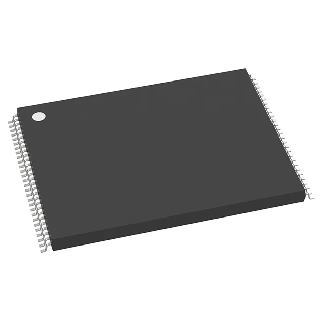
Infineon Technologies S29GL256P11TFI020 — Analog & Data Acquisition

S29GL256P11TFI020 256Mbit Parallel NOR Flash, 110 ns

MPNS29GL256P11TFI020
End of Life

Cypress GL-P series S29GL256P11TFI020, 256Mbit parallel NOR Flash, 110 ns access time, 2.7V-3.6V supply, 32M x 8 organization, -40°C to 85°C, 56-TSOP tray.

$9.82Ref. price · indicative, final on quote
Packaging56-TFSOP (0.724", 18.40mm Width)
StockContact for availability
MOQ1 pcs
  • 100% new & originalTraceable channels only — no refurbs, no pulls, no remarked parts.
  • Date & lot codes on quoteStated per line before you commit; label photos on request.
  • MSL-compliant ESD packingMoisture-sealed bags with indicator cards; reels photo-verified.
  • PayPal buyer protectionPay by T/T, PayPal or Payoneer — card payments covered end to end.

Specifications

S29GL256P11TFI020 Technical Specifications
ParameterValue
SeriesGL-P
Memory typeNon-Volatile
Mounting typeSurface Mount
Voltage2.7V ~ 3.6V
Memory interfaceParallel
Operating temperature-40°C ~ 85°C (TA)
PackageTray
TechnologyFLASH - NOR
Access time110 ns
Memory size256Mbit
Memory formatFLASH
Case56-TFSOP (0.724\", 18.40mm Width)
Memory organization32M x 8
Write cycle time - word, page110ns

Product details

256 Mbit parallel NOR Flash for code shadowing and data storage

The S29GL256P11TFI020 is a 256 Mbit parallel NOR Flash from the GL-P series, organized as 32M x 8. It has a 110 ns access time and operates from 2.7 V to 3.6 V.

110 ns access time — what it means for the bus

The 110 ns access time is the time from address assertion to valid data on the bus. The write cycle time (word/page) is also 110 ns.

56-TSOP package — rework and footprint

The part comes in a 56-TSOP package with a body width of 18.40 mm. It is a standard surface-mount footprint.

Active lifecycle — no LTB pressure

The S29GL256P11TFI020 carries an Active lifecycle status, meaning Cypress (now Infineon) still manufactures it. No last-time-buy notice has been issued, so the BOM line is stable for new designs and ongoing production. The part is ROHS3 compliant.

Frequently asked questions

What are equivalent parts for S29GL256P11TFI020?

Within the same GL-P family, the S29GL512T11TFIV20 is a 512 Mbit sibling with the same 110 ns access time but a 1.65 V core supply. For a lower-density option, the S29GL128S10TFIV13 offers 128 Mbit at 100 ns. Neither is a direct pin-compatible second source — verify the supply voltage and organization before substituting.

How to program S29GL256P11TFI020?

The device uses standard parallel NOR Flash programming commands — byte/word program, sector erase, and chip erase. A typical programmer (e.g., from Data I/O or BP Micro) handles the 56-TSOP footprint. The 110 ns write cycle time means page-mode writes can be used for faster programming.

Can S29GL256P11TFI020 replace S29GL256P10TFI020?

The S29GL256P10TFI020 is an earlier GL-P speed grade (100 ns). The S29GL256P11TFI020 is the 110 ns variant — slightly slower access time. If the controller can accommodate the extra 10 ns of read latency (e.g., by adding one more wait state), the parts are otherwise pin-compatible and functionally interchangeable.