128 Mbit parallel NOR flash for code shadowing and execute-in-place
The Infineon S29GL128S90DHI020 is a 128 Mbit parallel NOR flash memory from the GL-S series, organized as 8M x 16 bits. It is designed for embedded systems that need fast, random-access code storage — typically for execute-in-place (XIP) firmware, boot loaders, and configuration data in industrial controllers, networking gear, and automotive infotainment. The 90 ns access time defines the read cycle: the host controller can pull data every 90 ns in a page mode burst, which keeps the bus moving without wait states for most 16-bit MCUs and FPGAs at moderate clock speeds.
For a 16-bit wide memory, that translates to a maximum read bandwidth of roughly 22 MB/s in random access, higher in page or burst modes. This is fast enough to feed a 100 MHz ARM or RISC-V core without wait states if the flash is mapped into the code space, but a 200 MHz+ core will need a cache or a higher-speed serial flash. The write cycle time — 60 ns for word and page writes — is separate and governs programming speed; page writes let you load a buffer and commit in one cycle, which improves firmware update throughput.
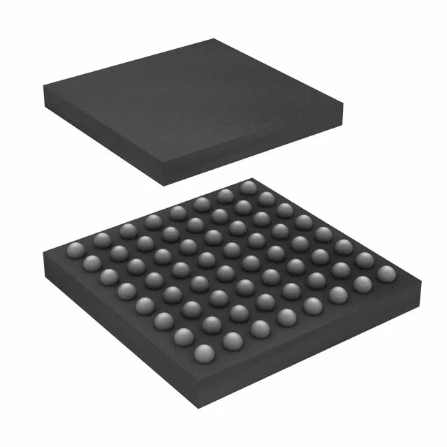
Package and footprint: 64-FBGA (9x9 mm)
The S29GL128S90DHI020 comes in a 64-ball Fine-Pitch Ball Grid Array (FBGA) package measuring 9 mm x 9 mm. The 0.8 mm ball pitch is standard for this density and is routable on a 4-layer board with via-in-pad techniques. The 64-LBGA footprint is shared with other GL-S density variants, so a board layout can be reused across 64 Mbit to 512 Mbit options without a respin.
The industrial temperature range is the most common specification for equipment that sees seasonal extremes but not under-hood heat. Storage temperature exceeds the operating range — handling and soldering, not running, is what that limit governs.
If you need a drop-in alternative, the S29GL128S10TFIV13 (100 ns access, same density and package) is a functional cross-reference — slightly slower, but pin-compatible and often available when the 90 ns grade is tight.