Infineon Technologies S29GL128S11FHIV20 — Memory (DRAM / SRAM / Flash / EEPROM)

S29GL128S11FHIV20 128 Mbit Parallel NOR Flash, 110 ns Access

MPNS29GL128S11FHIV20
Active

Infineon (Cypress) GL-S series S29GL128S11FHIV20, 128 Mbit parallel NOR Flash, 110 ns access time, 1.65 V supply, 8M x 16 organization, -40°C to 85°C, 64-FBGA tray.

$3.86Ref. price · indicative, final on quote
StockContact for availability
MOQ1 pcs
  • 100% new & originalTraceable channels only — no refurbs, no pulls, no remarked parts.
  • Date & lot codes on quoteStated per line before you commit; label photos on request.
  • MSL-compliant ESD packingMoisture-sealed bags with indicator cards; reels photo-verified.
  • PayPal buyer protectionPay by T/T, PayPal or Payoneer — card payments covered end to end.

Specifications

S29GL128S11FHIV20 Technical Specifications
ParameterValue
SeriesGL-S
Interface_typeParallel
Mounting_typeSurface Mount
Operating temperature high-40°C to 85°C (TA)
Frame_size128Mbit
Access time110 ns
Memory_typeNon-Volatile
Package_typeTray
Memory formatFLASH
Product_statusActive
Supply_voltage_v1.65
Memory organization8M x 16
Write cycle time - word, page60ns

Product details

128 Mbit parallel NOR Flash for code shadowing and execute-in-place

The Infineon S29GL128S11FHIV20 is a 128 Mbit parallel NOR Flash memory from the GL-S family, organized as 8M x 16 bits. It uses a standard parallel interface for direct code execution (XIP) and fast random-access reads, with a 110 ns access time that sets the bus timing budget for the host controller. The 1.65 V supply voltage lets it run from a single low-voltage rail, common in modern MCU and SoC systems where the I/O bank matches that level.

The 110 ns access time is the random-read latency from address assertion to valid data on the bus. For a 16-bit wide memory at 1.65 V, this timing determines whether the host controller can run back-to-back reads without wait states. The S29GL128S10TFIV13 sibling offers a 100 ns access time — a 10 ns improvement that may matter for higher-throughput systems, but for most 8/16-bit MCU designs the 110 ns part meets the margin. The write cycle time is 60 ns per word or page, which governs programming throughput during firmware updates.

64-FBGA footprint and supply routing

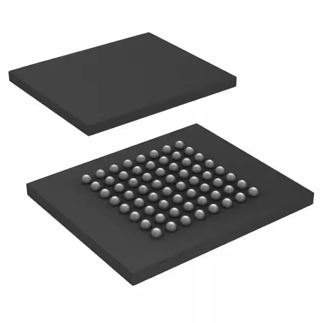
The 64-ball FBGA package (0.8 mm pitch typical for this class) requires a multilayer PCB with via-in-pad or dogbone fanout for the inner balls. The 1.65 V supply rail should be decoupled with a 100 nF ceramic per supply ball group, placed as close to the balls as the fanout allows. The parallel interface uses separate address, data, and control lines — route them with matched trace lengths to avoid skew at 110 ns cycle times.

Frequently asked questions

What is the difference between S29GL128S11FHIV20 and S29GL128S10TFIV13?

The S29GL128S10TFIV13 has a 100 ns access time versus 110 ns for this part, and it ships in Tape & Reel packaging instead of tray.