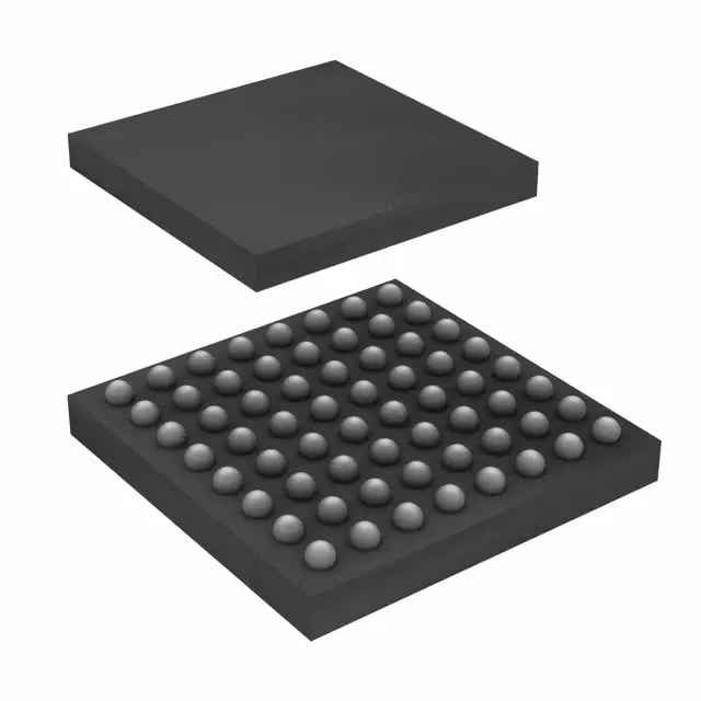
Infineon Technologies S29GL128S10DHB020 — Discrete Semiconductors

Infineon S29GL128S10DHB020 NOR Flash, 128Mbit, 100ns

MPNS29GL128S10DHB020
End of Life

Infineon Technologies GL-S series Automotive AEC-Q100 NOR Flash, S29GL128S10DHB020, 128Mbit, 100ns access, 2.7-3.6V, Parallel, -40 to +105°C, 64-FBGA (9x9), Tray.

$7.56Ref. price · indicative, final on quote
Packaging64-LBGA
RoHSROHS3 Compliant
SeriesAutomotive, AEC-Q100, GL-S
Sourced new & surplus through independent channelsAuthenticity-screened · ESD-safe packingListing updated Aug 2026

Specifications

S29GL128S10DHB020 specifications
ParameterValue
SeriesAutomotive, AEC-Q100, GL-S
Memory typeNon-Volatile
MountingSurface Mount
Voltage2.7V ~ 3.6V
Memory interfaceParallel
Operating temperature-40°C ~ 105°C (TA)
PackageTray
TechnologyFLASH - NOR
Access time100 ns
Memory size128Mbit
Memory formatFLASH
Case64-LBGA
Memory organization8M x 16
Write cycle time - word, page60ns

Product details

128 Mbit parallel NOR flash for automotive code storage

The Infineon S29GL128S10DHB020 is a 128 Mbit parallel NOR flash memory from the Automotive GL-S series, organized as 8M x 16 bits.

Access time and write-cycle budget

With a 100 ns access time, this part supports zero-wait-state reads from a 10 MHz bus clock and can stretch to higher frequencies with a single wait state inserted by the memory controller. The 60 ns write cycle time (word/page) means a full 128-word page buffer fills in under 4 µs, which then programs in a single embedded algorithm cycle — useful for OTA firmware updates where the total write time is dominated by the page program sequence, not the bus transfer.

Package and board integration

Housed in a 64-ball FBGA (9x9 mm) package, the 0.8 mm ball pitch allows a 4-layer PCB with microvias to fan out all signal and supply balls without blind vias.

RoHS3 compliant (2011/65/EU + 2015/863). The AEC-Q100 qualification includes the full Grade 1 temperature sweep and reliability stress sequence — the part ships with lot traceability and the manufacturer's standard warranty through authorized distribution.

Frequently asked questions

What is the memory organization of S29GL128S10DHB020?

128 Mbit organized as 8M x 16 bits. The parallel interface reads and writes 16-bit words directly, so a 16-bit MCU bus maps the full density without byte-lane multiplexing.

Can S29GL128S10DHB020 replace an FM28V102A-TG FRAM in an existing design?

No — the FM28V102A-TG is a 1 Mbit FRAM with a different pinout, supply voltage (2.0 V), and temperature range (85°C max). The S29GL128S10DHB020 is 128x denser and runs at 3.3 V with a wider temp range, but the two are not pin-compatible or drop-in replaceable. A board spin and firmware change would be required.