What this NOR Flash does on the board
The Infineon S29GL128P11FFIV10 is a 128 Mbit parallel NOR Flash memory from the GL-P series, organized as 16 M x 8 bits. It stores boot code, firmware images, or configuration data for embedded systems that need fast, random-access reads and reliable non-volatile storage. The parallel interface means the host — typically an MCU, FPGA, or SoC — reads and writes through a dedicated address and data bus, giving deterministic access without the protocol overhead of SPI or Quad-SPI. The 110 ns access time sets the bus wait-state budget; a 48 MHz ARM core, for example, inserts one or two wait states to match the flash read timing.
110 ns is the random-access read time from address latch to valid data out. For a system clocked at 50 MHz (20 ns period), that's about 5.5 bus cycles before the host can sample the data. A memory controller with programmable wait states handles this cleanly; a fixed-state machine may need a clock divider or a slower bus speed. The write cycle time — word or page — is also 110 ns, so program operations complete at the same rate as reads. If you're replacing an older 90 ns or 100 ns parallel flash in a legacy design, the 110 ns part may add one extra wait state. Verify the controller's timing budget before dropping it into a tight bus. The GL-P series is pin-compatible across density options, so a 128 Mbit swap for a 64 Mbit or 256 Mbit sibling usually needs only a board spin for the extra address lines.
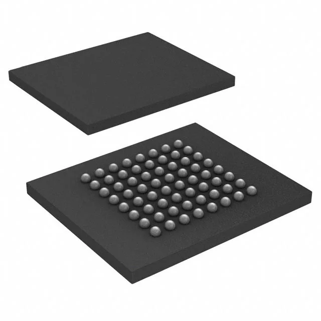
The S29GL128P11FFIV10 comes in a 64-ball LBGA with a 13 x 11 mm body. Surface-mount only.