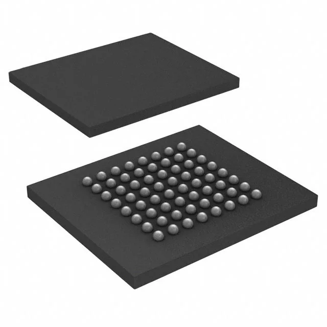
128 Mbit parallel NOR flash for firmware storage
100 ns access time — bus timing compatibility
The 100 ns access time is the key timing parameter for this part. It defines how quickly the flash outputs valid data after the host asserts the address and chip enable. For a host controller running at 10 MHz or slower, this is comfortable; at higher bus speeds you may need to insert wait states or use a faster part. The write cycle time — word and page — is also 100 ns, so page-mode programming (typically 32 words per page) completes in a few microseconds. Compare this to the S29GL128S10TFIV13, which has the same 100 ns read access but a 60 ns write cycle time, giving faster page writes for firmware-update-heavy applications.
That means it is still in regular production with no announced end-of-life or last-time-buy. The GL-P series has been a workhorse in industrial and communications equipment, and Infineon continues to support it alongside the newer GL-S and GL-T families.
Package and footprint — 64-FBGA (13x11 mm)
Housed in a 64-ball Fine-Pitch Ball Grid Array (FBGA) measuring 13x11 mm, this flash mounts on the PCB with a standard 0.8 mm ball pitch. The package is RoHS3 compliant and lead-free. When laying out the board, keep the parallel bus traces length-matched and decouple the supply pins with a 100 nF ceramic per Vcc pin — the datasheet recommends a 4.7 µF bulk capacitor near the flash as well.