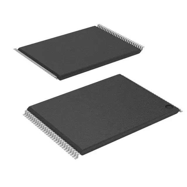
1 Gbit parallel NOR flash for code-shadowing and data-logging
The Infineon S29GL01GT11TFIV40 is a 1 Gbit parallel NOR flash from the GL-T series, organized as 128M x 8 bits. It uses a parallel interface, which means the address and data buses are separate — the CPU reads or writes the flash in a single bus cycle, unlike serial flash that shifts data out bit by bit. This matters when the processor boots directly from flash or executes code in place (XIP), because the parallel bus delivers the first instruction with deterministic latency. The 1.65 V supply rail aligns with low-power SoC cores and FPGAs that run their I/O bank at 1.8 V nominal — no extra level translator between the flash and the host memory controller.
The 110 ns access time is the time from when the address is valid on the bus until the data appears at the output pins. In a system with a 100 MHz memory controller (10 ns clock period), the flash needs 11 clock cycles to return the first word. That is fine for boot code and firmware storage, but the controller must insert wait states — the flash does not handshake; the designer programs the number of wait states into the memory controller's timing registers. Page-mode and word-program timing is 60 ns for the write cycle, which governs how fast the CPU can program a word or a page after the initial command sequence. Bulk firmware updates over a slow fieldbus (CAN, RS-485) are gated by the bus speed, not the flash write time; the 60 ns page program is fast enough that the bottleneck stays on the communication link.
Because it is active and widely used, the part is sourced against an RFQ from authorized and independent channels.