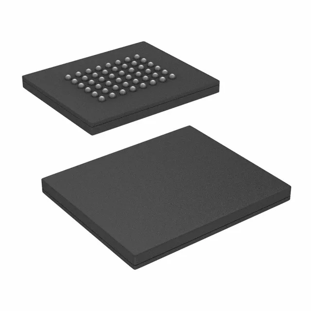
Infineon Technologies S29AL016J70BFI012 — Discrete Semiconductors

S29AL016J70BFI012 16Mbit Parallel NOR Flash, 70 ns, 48-FBGA

MPNS29AL016J70BFI012
End of Life

Infineon Technologies AL-J series parallel NOR flash, S29AL016J70BFI012, 16Mbit, 70 ns access, 2.7-3.6 V, -40 to +85°C, 48-VFBGA package.

$2.71Ref. price · indicative, final on quote
Packaging48-VFBGA
StockContact for availability
Lead time3-5 Days wk
MOQ1 pcs
  • 100% new & originalTraceable channels only — no refurbs, no pulls, no remarked parts.
  • Date & lot codes on quoteStated per line before you commit; label photos on request.
  • MSL-compliant ESD packingMoisture-sealed bags with indicator cards; reels photo-verified.
  • PayPal buyer protectionPay by T/T, PayPal or Payoneer — card payments covered end to end.

Specifications

S29AL016J70BFI012 Technical Specifications
ParameterValue
SeriesAL-J
Memory typeNon-Volatile
Mounting typeSurface Mount
Voltage2.7V ~ 3.6V
Memory interfaceParallel
Operating temperature-40°C ~ 85°C (TA)
PackageTape & Reel (TR); Cut Tape (CT)
TechnologyFLASH - NOR
Access time70 ns
Memory size16Mbit
Memory formatFLASH
Case48-VFBGA
Memory organization2M x 8, 1M x 16
Write cycle time - word, page70ns

Product details

48-FBGA footprint and board integration

The S29AL016J70BFI012 comes in a 48-VFBGA package with a 8.15x6.15 mm body (48-FBGA). The 0.50 mm ball pitch demands a controlled-impedance breakout on a 4-layer board; the inner layers carry the address and data bus routing to the host controller without via stubs that would reflect the 70 ns access edge. Surface-mount assembly with the standard JEDEC moisture sensitivity level for thin FBGA packages — bake before reflow if the floor life has been exceeded. The 48-ball array distributes the I/O, supply, and ground pins evenly, so the decoupling capacitors sit directly under the package on the opposite side of the board.

16 Mbit parallel NOR with 70 ns access

Organised as 2M x 8 or 1M x 16 via the byte-wide select pin, the 16 Mbit array is accessed through a full parallel address/data bus. The write cycle time per word or page is 70 ns, matching the read access, so the firmware update routine does not need separate timing parameters for program operations.

Active lifecycle and compliance

The AL-J series is a mature parallel NOR flash family with a long production history.

Frequently asked questions

What is the memory organization and interface of S29AL016J70BFI012?

The 16 Mbit array is organised as 2M x 8 or 1M x 16 with a full parallel address/data interface. Random read access time is 70 ns.