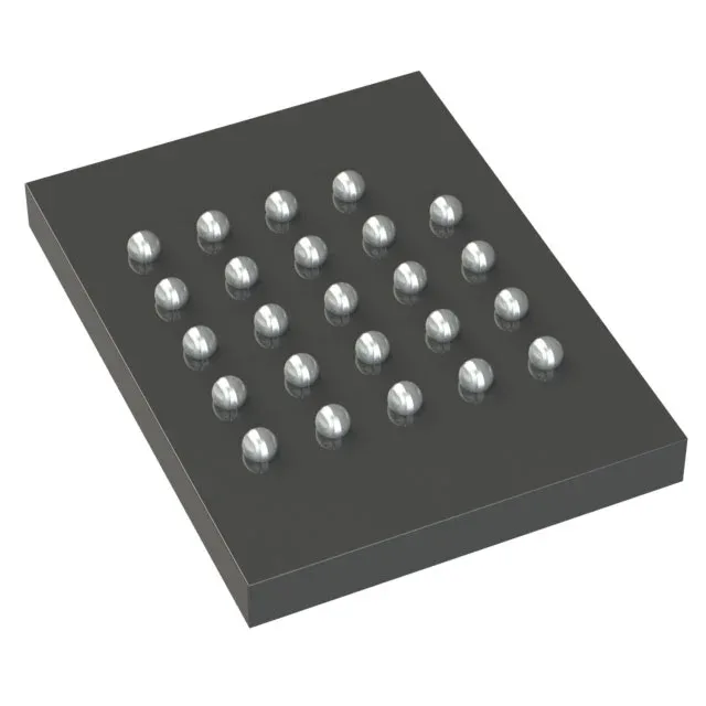
Infineon Technologies S26KS512SDPBHN020 — Memory (DRAM / SRAM / Flash / EEPROM)

S26KS512SDPBHN020 512Mbit HyperFlash™ KS NOR Flash, 166 MHz

MPNS26KS512SDPBHN020
Active

Cypress HyperFlash™ KS S26KS512SDPBHN020, 512Mbit parallel NOR Flash, 96 ns access time, 166 MHz clock, 1.7 V supply, -40°C to 125°C TA, 24-FBGA.

$14.78Ref. price · indicative, final on quote
StockContact for availability
MOQ1 pcs
  • 100% new & originalTraceable channels only — no refurbs, no pulls, no remarked parts.
  • Date & lot codes on quoteStated per line before you commit; label photos on request.
  • MSL-compliant ESD packingMoisture-sealed bags with indicator cards; reels photo-verified.
  • PayPal buyer protectionPay by T/T, PayPal or Payoneer — card payments covered end to end.

Specifications

S26KS512SDPBHN020 Technical Specifications
ParameterValue
SeriesHyperFlash™ KS
Interface_typeParallel
Mounting_typeSurface Mount
Operating temperature high-40°C to 125°C (TA)
Frame_size512Mbit
Access time96 ns
Memory_typeNon-Volatile
Frequency_hz166000000.0
Package_typeBulk
Memory formatFLASH
Product_statusActive
Supply_voltage_v1.7
Memory organization64M x 8

Product details

512 Mbit HyperFlash™ KS — what the specs mean for your design

The Cypress S26KS512SDPBHN020 is a 512 Mbit parallel NOR Flash from the HyperFlash™ KS family, organized as 64M x 8. It delivers a 96 ns initial access time and supports a 166 MHz burst clock, making it a strong candidate for execute-in-place (XIP) code storage in high-reliability embedded systems. The 1.7 V supply rail lets it run from a single-cell battery or a modern low-voltage core supply without a separate regulator. The 24-ball FBGA package keeps the footprint compact for space-constrained PCBs, but the BGA requires careful rework planning — a hot-air profile that reaches the center balls without overheating the surrounding passives is essential.

Parallel interface — bus timing and layout

The parallel interface (address/data multiplexed) ties directly to a host memory controller with a dedicated chip select and read/write strobes. The 96 ns access time sets the minimum read cycle for random access; at 166 MHz burst mode, the controller can stream sequential instructions at full clock rate. On the PCB, keep the parallel bus traces length-matched and avoid vias on the data lines to maintain signal integrity at this speed.

Frequently asked questions

Can S26KS512SDPBHN020 replace S26KS512SDPBHN010?

The S26KS512SDPBHN020 and S26KS512SDPBHN010 share the same 512 Mbit density and HyperFlash™ KS family, but the suffix difference may indicate a package or temperature variant. Confirm the exact suffix mapping against your BOM's approved vendor list before substitution.