96 ns access time and 133 MHz burst — what they mean for XIP
The 96 ns random access time sets the latency for the first read after a row change; in an execute-in-place (XIP) firmware boot, this is the time from address assertion to data valid on the bus. Once the page is open, the 133 MHz clock sustains sequential reads at the full bus rate, so the bottleneck shifts from the Flash to the memory controller. For a 512 Mbit density, the 64M x 8 organization means each byte lane carries one-eighth of the total storage, which simplifies the PCB routing for a 16-bit or 32-bit host interface.
AEC-Q100 and 105°C — qualification scope
The 105°C upper limit is the ambient temperature at which the device is guaranteed to meet all AC/DC specifications — relevant for ECUs mounted on the engine block or in the transmission tunnel. The 1.7 V supply rail is common in modern automotive SoC domains; the part will hold data down to the minimum operating voltage without a brown-out reset.
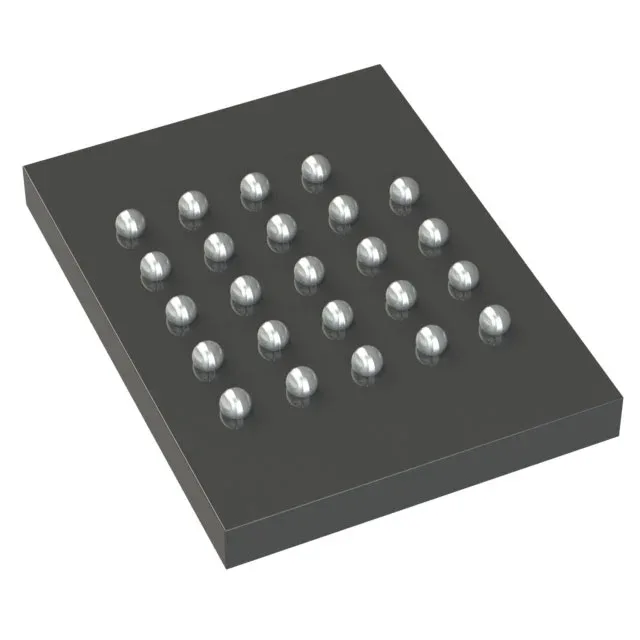
Infineon lists the S26KS512SDGBHB030 as Active. The 24-ball FBGA package (0.8 mm pitch, 6 x 8 mm body) is a common footprint shared across the HyperFlash™ KS density range, which simplifies board layout reuse if a smaller or larger density is needed later.