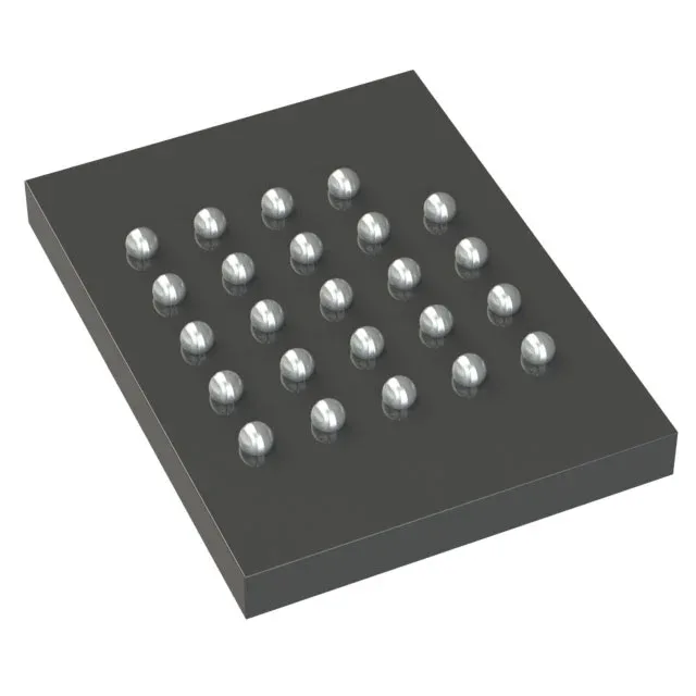
HyperFlash™ KS — 256 Mbit parallel NOR Flash for real-time execution
The Infineon S26KS256SDABHV030 is a 256 Mbit parallel NOR Flash from the HyperFlash™ KS family, organized as 32M x 8 bits. It's built for direct code execution — XIP (eXecute-in-Place) — where the MCU or FPGA fetches instructions straight from Flash without copying to RAM first. The parallel interface keeps read latency low, and the 96 ns access time means the first word appears on the bus within that window after the address is strobed. After that initial access, the 100 MHz burst clock sustains sequential reads at the full bus rate. The supply voltage is 1.7 V, which puts this part squarely in the 1.8 V logic domain — common on modern SoCs and FPGAs that run their I/O banks at 1.8 V.
The 96 ns access time is the random-read latency: from the moment the controller asserts the address, the first data word is valid on the bus 96 ns later. For a 100 MHz bus (10 ns period), that's roughly 9.6 clock cycles of wait states before the first read completes. After that, the burst mode feeds subsequent words at the 100 MHz rate — one word per cycle. Compare this to a traditional asynchronous parallel NOR like the S29GL512T11TFIV20, which has a 110 ns access time and no burst mode: the HyperFlash KS pulls ahead on sustained throughput once the initial latency is paid.
The 125°C ceiling matters for engine-bay electronics, exhaust-side sensors, or any sealed enclosure where internal ambient can push past 105°C. The sibling S26KS128SDPBHV020 only goes to 105°C, so if your thermal analysis shows junction temperatures above that, the S26KS256SDABHV030 is the one that stays within spec.
If you need a second-source candidate, the S26KS128SDPBHV020 is the same HyperFlash KS family at half the density (128 Mbit) and a 105°C temperature ceiling — same 96 ns access time, same 1.7 V supply, same 24-FBGA footprint. It's a drop-in for designs that don't need the full 256 Mbit or the 125°C rating.