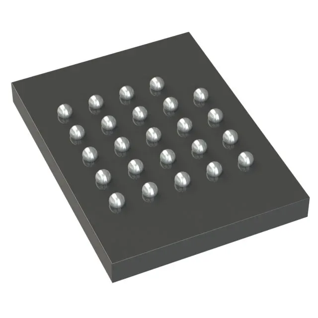
128Mbit parallel NOR flash in a 24-ball FBGA
The S26KS128SDABHV030: It delivers a 96 ns initial access time and supports a 100 MHz clock for page and burst reads — the parallel interface keeps the memory controller simple, with no serial protocol overhead on the bus. The 24-ball FBGA package (0.80 mm pitch, roughly 6 x 8 mm body) demands a controlled-impedance layout on the parallel data and address lines — the datasheet's layout guide on page 12 recommends keeping trace lengths matched within 25 mm across the byte lane.
Access time and frequency — what they mean for read throughput
The 96 ns initial access is the random-read latency from the first address strobe to valid data on the bus. For sequential reads, the 100 MHz clock delivers a 10 ns cycle — after the first word, subsequent words in the same page appear every 10 ns, so a 32-byte burst finishes in under 400 ns. This matters for code execute-in-place (XIP) where the CPU fetches instructions directly from flash: the initial access sets the first-instruction latency at reset, while the page mode sustains the throughput for linear code execution. The 1.7 V supply is the minimum operating voltage — the nominal range is 1.7 V to 2.0 V per the HyperFlash family spec. At 1.7 V the internal charge pump still generates the program/erase voltage, but the read current is lower than at 1.8 V. Derate the access time by about 5 ns at the low end of the voltage range; the datasheet's AC timing table (page 22) lists the conditions.
Active production — sourcing and compliance
Infineon lists the S26KS128SDABHV030 as Active.