512 Mbit parallel NOR — the density and the bus
The S26KL512SDABHV020 is a 512 Mbit parallel NOR flash from Infineon's HyperFlash™ KL family, organized as 64M x 8 and accessed through a parallel interface. The 96 ns access time sets the random-read latency the host controller sees on the first word; after that, the 100 MHz clock drives the synchronous burst for sequential code execution or data streaming.
Industrial temperature and active lifecycle
The 105°C ceiling is the junction limit for sustained operation, not a transient peak. Infineon lists this part as Active.
Parallel bus vs SPI — the footprint decision
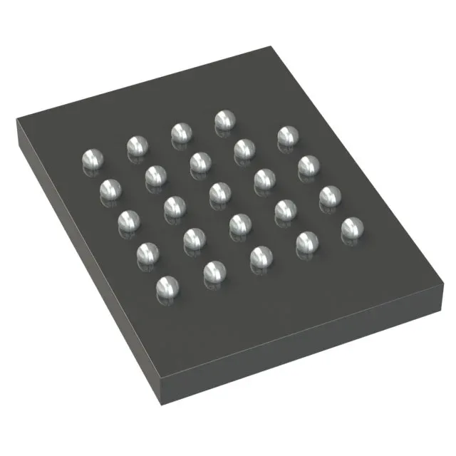
The parallel interface distinguishes this part from the SPI NOR flash that dominates many embedded BOMs. The 24-FBGA pinout and the 8-bit data bus require a different PCB layout than a serial-flash footprint — a board spun for the S25FL512SAGMFBG10 (SPI Quad I/O) cannot accept this part without a re-spin. The trade-off is higher read throughput per clock cycle vs fewer board traces. Within the HyperFlash family, the S26KS128SDPBHV020 shares the same 24-FBGA package but runs at 1.7 V core and packs 128 Mbit — one-quarter the density. The pinout is compatible, but the supply rail difference (2.7 V vs 1.7 V) means the board must support both voltages if a density swap is planned. No drop-in replacement without a rail change.