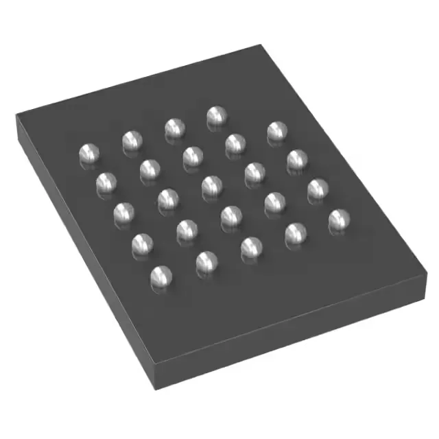
Package and board-fit — 24-BGA footprint
The S25HS512TFABHI010 comes in a 24-ball BGA (8x6 mm body) — the 0.80 mm ball pitch is standard for a 4-layer board; the outer rows fan out without microvias, but the inner rows need a via-in-pad or a dogbone breakout if the trace width and spacing are tight. Supply voltage is 1.7 V to 2.0 V, so the core rail must stay within that window at the BGA balls — the IR drop across the PCB trace from the regulator output to the flash VDD ball should be under 50 mV at the peak read current to avoid brownout at the low end.
Memory density and interface — 512 Mbit via SPI/Quad I/O
512 Mbit organized as 64M x 8 — the Quad SPI interface reads at 166 MHz, delivering a theoretical throughput of 664 Mbit/s in quad mode, which is enough for code shadowing or data logging without a parallel bus. The 166 MHz clock rate is the ceiling for the SPI bus — the actual throughput depends on the controller's SPI peripheral and the PCB trace length; a 10 cm trace at 166 MHz starts to show signal-integrity loss unless the impedance is controlled.