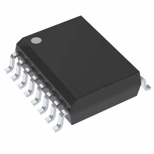
It uses the SPI Quad I/O interface, which allows four data lines for read operations at a 66 MHz clock, delivering faster throughput than standard SPI while keeping the pin count low — a practical choice for embedded systems that need a large code or data store without a parallel bus footprint.
66 MHz clock and Quad I/O — read throughput in practice
At 66 MHz with Quad I/O, the effective read throughput is about 33 MB/s in fast-read mode. That is enough for direct code execution (XIP) from NOR Flash in many MCU and SoC designs, as long as the host controller supports Quad I/O. The 512 Mbit density (64 MB) holds a full firmware image plus a file system or configuration tables, with room for OTA update staging. For designs that need higher throughput, a DDR Quad I/O part would be the next step, but this part keeps the pin count at six signals (plus chip select) — a fair trade-off for a 16-SOIC layout.
The FL-S series is a mature, broadly adopted family, so PCN risk is low relative to a niche or recently introduced part.
Package and mounting — 16-SOIC wide-body
It uses a gull-wing lead form, which is straightforward to inspect and rework. The package is rated for standard reflow profiles (MSL 3 typical for this class — verify the specific moisture sensitivity level from the lot date code). For layout, keep the SPI signal traces short and matched for the 66 MHz clock rate, and place a 100 nF decoupling capacitor within 2 mm of each VDD pin.